Archive
What needs to be done to boost chip designing activities in India?
 Anil Gupta, Technovation 2010 and UK CIG Convener, India Semiconductor Association (ISA), also needs no introduction. As former managing director, ARM Embedded Technologies Pvt. Ltd, he has been a prominent figure in several industry events. Here, he presents his views on what needs to be done for the Indian semiconductor industry.
An interesting fact being brought up time and again within the industry is the requirement of a robust entrepreneurial spirit and the need for much more sources of funding for semiconductor product companies. Also, renewable energy, healthcare and security are some of the verticals where the Indian industry believes there is a lot of value to be added from the Indian market/need perspective.
Further, local products/systems design and development activity needs to be encouraged and kick-started in a big way in India, for the industry to really succeed big time!
What does Indian semicon need?
We have discussed several times in the past regarding what needs to be done with the Indian semicon industry. So, what really needs to be done, given the current slowdown? What can be done boost chip designing activities in India.
According to Anil Gupta: “The Indian story has always been a story of a lot of potential, but most often this potential is never realized.
“The software industry has done well and has gone far, perhaps, somewhat farther than the hardware or chip-design industry in India. However, you still don’t see a software product conceptualized, designed and developed in India that is worth mentioning.
“The Infosys’es and the I-Flex’es can do a phenomenal job of executing software projects for their customers, but they are all a far cry from the league of the top consulting firms that define the problem to be solved and the software solutions to be built.
“The Indian software industry is still plagued with the “revenue per head” model and is unable to grow beyond it. The Indian software companies clearly bring a significant value to their customers but this is NOT strategic value, it is merely an execution value.
“Compared with the software industry, the embedded systems industry in India is puny today. However, the opportunities are phenomenal because there is so much automation potential in so many verticals. However, once again, the lack of significant products/solutions development in India is a very big hindrance.”
From a technical expertise perspective, there is a lot of engineering talent available, but the expertise is in general quite shallow. Even in the open source space like Linux, there aren’t many noteworthy contributions to date from the Indian engineering community.
Is the Indian fab story truly dead and buried?
In the past, we have extensively discussed whether the Indian fab story was dead and buried. Do you see any change in the current situation?
Well, it is dead for now! Gupta added: “Its day will come ONLY when the economics works out in its favour. Today, it doesn’t!”
He said: “It is interesting that many point out to the success of the solar fab investments. However, it should be noted that there is no solar wafer manufacturing activity worth mentioning. Only modules are being assembled in India as there seems to be a global glut in wafer production. Thus, wafer fabs in India is a pipe dream for now since the economics doesn’t work out.”
Does India have entrepreneurs committed to product development and willing to take that risk? How can they be encouraged?
Gupta said that there are not that many who are willing to come out and take the risk, and the lack of funding is a very big handicap. The lack of prior successes that could be emulated is probably the biggest handicap.
In that case, what needs to be done in India to move up a higher level, beyond design and verification?
He said: “Clearly, a willingness to take risk, strong stomach to face failure, and strong will to learn from that failure to rise again from the ashes!”
Intel's margins hurt again by Atom to tune of $1bn
Intel’s misjudgment of the low margins of the Atom in its netbook processor has hurt the company for the second successive quarter, according to the report: “Netbook-Mobile Internet Device Convergence: Strategic Issues and Markets,” recently published by The Information Network (www.theinformationnet.com).
The Information Network had stated on January 7 that Intel misjudged the success of the Netbook and its Atom processor to the tune of about a billion dollars for Q4. Given the low margins announced in its Q1 release, Intel is still bogged down by the Atom.
The Atom used in a Netbook is processed with 45nm feature sizes on 300mm wafers and measures 25sqmm. It is priced at about $29. Intel’s Penryn Core 2 processor is used in Notebooks. It is also processed with 45nm feature sizes on 300mm wafers and measures 107sqmm. It is priced at about $279. There is a price difference of $200 per processor between the Penryn and Atom, but more importantly, a difference of $115,000 per processed 300mm wafer.
“Intel rethought its production schedule in Q1 by allocating capacity for the Atom and for the Penryn, unlike Q4 where the cut back production on the more profitable Penryn,” noted Dr. Robert N. Castellano, president of The Information Network. “We estimate that Intel produced 5 million Atom processors and 50 million Penryns.”
On March 2, Intel and TSMC announced they had reached an agreement to collaborate on technology platform, IP infrastructure, and SoC solutions for the Atom CPU cores. That situation will improve Intel’s margins for Q2 2009.
“While the announcement was slated toward TSMC’s capability to produce Atom cores for Intel’s march into the Mobile Internet Device (MID) market, which is dominated by ARM, it was an opportunity for Intel to wipe production of the Atom off its books. I’d like to think of it as ‘Intel’s Atom Bomb’,” added Dr. Castellano. “It indicates the tech sector is not really that bad off as the numbers suggest, but just a miscalculation on Intel’s part. Indeed, Intel did say that the bottom had been reached in the PC sector.”
ISA Vision Summit 2009: Growing influence of embedded software on hardware world
This session on day 1 of the recently held ISA Vision Summit had a good mix of speakers. Moderated by Anil Gupta, managing director, ARM India, the speakers included V.R. Venkatesh, Senior Vice President, Product Engineering Services, Wipro Technologies, Kishor Patil, MD & CEO, KPIT Cummins, and Raju Pudota, MD, Denali Software. This is a slightly longer blog post, so bear with me, friends.
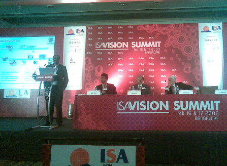 The pic here shows Wipro’s Venkatesh making a point, watched by Raju Pudota, Amil Gupta and Kishor Patil.
Kicking off the panel discussion, ARM’s Anil Gupta highlighted the strength of the Indian embedded software industry. As per IDC, embedded software accounts for 81 percent of the projected share of overall revenues in 2008, at $5.98 billion. This will go up to $7.29 billion, while still accounting for 81 percent of the projected share of overall revenues in 2009. The projected share of the overall workforce in this industry segment stands at 82 percent — at 125,663 — which will be maintained during 2009, even as this figure rises to 149,978! Quite impressive!!
Incidentally, a recruiter recently requested information on the workforce numbers in the Indian semiconductor industry. I hope this partly answers your question, friend.
Gupta further added that embedded design had now entered several sectors such as automotive, aerospace and defense, consumer and home products, household appliances, industrial controls, infrastructure and construction, medical electronics, transportation and traffic management, security and telecom. In short, a bright future for this segment ensured, especially in India.
Trends in embedded design include: more demand for features, embedded is driving complexity, and prices have been generally constant/going down. As a result, all of the innovation happening has been giving new experience to the consumers.
Wipro’s V.R. Venkatesh cited the example of medical devices, which are adding functions via embedded software. He presented the case of an efficient infusion pump, which ensures that the five rights of medication safety — right person, right dose, right medicine, right time, and right way — are never violated!
Another example cited was of adding functions in mobile devices. Such mobile devices are making use more dual core chip solutions to run multimedia and MIPS intensive apps on a separate applications processor. They use open operating systems (OS) such as Symbian, Linux, etc., and also have built in sensors, such as motion sensors.
Consequently, usability is now becoming the focus, rather than pure user interface of the mobile. On the impact of software complexity, he said that OSs and middleware are now becoming more complex to enable quicker and easy to develop mobile applications, and also develop complex mobile application with the right API support. He also cited new advances in automotive telematics and navigation. These are implemented through complex software and demanding more hardware features.
Challenges in developing embedded software
However, increasing embedded software has also brought its own challenges. Today, the share of software is ~50 percent of the total cost of development.
Some of the challenges while developing embedded software include multiple regulations; split personality: display (local and remote), compute and communicate; UI; low-power design, application specific accelerators; wireless as de facto connectivity; integrated sensors and geospatiality for enhanced applications; built for untrusted environments (security, virtualization); and integration with service providers and enterprise systems.
Hardware and software in an embedded system are complimentary to each other. Software (middleware and applications) should be used as a ‘Differentiator’ to add more winning features to any new product, he added. There is a need for a platform approach for embedded software development to enable scaling of features and usage across applications. Finally, developers need to keep the cost vs. functions vs. efficiency tradeoff in mind.
Embedded systems landscape trends
KPIT Cummins’ Kishor Patil touched upon the growing need of convergence for hardware and software. According to him, the key driving forces are:
* Low cost and high performance;
* Low power and green;
* Maximum storage and least area/cost;
* Development: Faster TAT (turnaround time);
* Mechanical centric => electronics centric; and
* High value and low cost.
Trends in hardware include silicon shrink at 0.7x, technology challenges at 45nm and below, and business challenges — high volumes for amortizing high mask costs.
Commenting on the embedded systems landscape: market trends and implications, he cited these to be: electronics and applications emerging as distinctive factors; increased electronics in automobiles (~100 MCUs/ECUs per car); silicon shrinkage reaching its limit w.r.t. geometry and costs; and enhancing system performance with the same hardware.
Content growth has been quite notable in automotive electronics. According to Patil, in 2000, an average automobile had 1 million lines of code, 20 ECUs, electronics worth $400, and software constituted 2 percent of the cost of the car. By 2010, an average car will have 100 million lines of code, 50 ECUs, electronics worth $1,100 and software cost at 13 percent of the cost of a car. Of this, 50 percent will be infotainment and 30 percent will be power train.
Impact on stakeholders
So what is the impact on the stakeholders? For OEMs, tier 1s, and semicon companies, it brings new business opportunities, and application specific solutions — common/configurable hardware differentiated by software.
It allows R&D to migrate from proprietary interfaces to open and standard-based interfaces. The impact on software developers includes use of heterogeneous processors, managing parallelism, as well as dealing with scalability, compatibility and re-usability.
Embedded software’s growing importance
Denali’s Raju Pudota focused on current trends, such as growth in UMPC (ultra mobile PCs) designs; multimedia and automotive. For hardware, it means higher integration, multiple embedded processors in one SoC, and multiple microcontrollers (MCUs) with independent functions. Most importantly, embedded software is needed to make all of this work!
He said that more software is required to run all of the IPs integrated on the chip. These can be procured from hardware IP vendors, or developed in-house or contracted to third party providers. Also, different processors require different skills and capabilities. Finally, integration and embedded OS level capabilities. Incidentally, embedded software has become a requirement on the semicon provider. However, third-party IP has been evolving slowly.
Semicon providers’ activities are manifold. These involve developing software for in-house hardware components, sourcing software from hardware IP providers, integrating various software components, and also test software offered to the system integrator.
These growing activities present its own challenges, typically: quality of software provided by hardware IP vendors, high integration time, software verification, and increased investment in software capabilities — and emergence of a new area of core competence.
What can the ecosystem do?
Given this scenario, the ecosystem has a major role to play. These include:
Ease of generation of hardware-aware software — define methods to abstract design to enable auto-generation of device drivers; define methods to auto-generate device drivers; few companies investing in this area.
Define framework/platform to integrate software — similar to on-chip interconnect; leverage mature general software development processes; and customize to specific requirements of embedded area. Finally, make software offerings open-source; leverage large independent developer community.
Ease testing of embedded software
There is also a need to ease the testing of embedded software. Some points to note: Leading semicon providers have home grown software integration and testing platforms; making use of traditional methods — hardware-software co-simulation, simulation acceleration, emulation, and FPGA testing. However, no standard methodology is said to be evolving.
Many industry solutions currently exist for hardware-software integrated testing, such as CoWare, SystemC, Mirabilis, etc. Then, there’s also simulation accelerators (parallel processing), and emulators (FPGA based).
Challenges include: huge investment in model development, high cost of ownership, the ability of third party IP provider to enable integration, and large turnaround time per test. A proper framework for the integration and testing of IPs and embedded software is the need of the hour.
Pudota added that while this is a tough challenge, it would improve time-to-market for complex SOCs, develop a third-party IP ecosystem, and enable the semicon provider to focus on core competencies.
Indian silicon wafer fab story seems dead and buried! Should we revive it?
Now then, this will make a very interesting read! Back in October 2007, I had discussed the timing and the need for a silicon wafer fab in India, in-depth, with Anil Gupta, managing director, India Operations, ARM.
 We have come a long way since then! There was all the hype last year about SemIndia’s fab, which never really did happen, and eventually, BV Naidu moved on! Then came the rush to solar fabs. Recently, when I blogged on how a Qimonda buy could be good for India, I am told that it is really outrageous. No problem, it is merely a suggestion.
At times, I have got the feeling whether the Indian semiconductor industry is losing its way! However, when I see all around, it is hale and hearty, and business as usual — fabs or no fabs!
It was interesting to meet up again with Anil Gupta of ARM, and to find out what he thought about what I thought!
Starting with an old question, whether India has the capability to sustain or even build a product development ecosystem? Gupta said: “We need the following for this:
* Entrepreneurs committed to product development and willing to take that risk.
* Investors willing to take risk on product development companies.
* Consumption (this will happen as the economy improves any way).
* Deep enough technical/technological knowledge/know-how to put reasonably competent end products together (It exists. Examples like Sukam, Tejas and other are there).
Indian fab story dead and buried
Turning focus on fabs, is the Indian silicon wafer fab story completely dead and buried now? Gupta notes: “When TSMC says they are running at only 38 percent capacity, one can imagine what the rest of the fabs must be going through. In any case, the Indian fab story was a longer term story and the current economic climate actually makes it further and further remote. So yes, it is dead and buried now!”
Wow! India probably flattered to deceive! However, I am an optimist, and hope that one day, India will have its own silicon wafer fabs!
Gupta adds: “What worries me now is the glut of the solar/PV fabs. By the industry estimates, solar/PV is a viable option only when the price of oil is >$100 per barrel (oil is at $40 per barrel now). This means, there would be challenges for the solar cell industry too! One can only hope that the economy picks up growth soon enough and sends the price of oil higher so that solar becomes a viable option.”
Again, this is a concern I have as well. The rush toward solar is good, but then, is this what the Indian semiconductor industry really needs? Where’s all that talk of developing silicon and product companies? You simply cannot equate the two — semicon and solar! You can’t have a policy, and then ignore the main crux either, and simply go for the ones that are easily attainable! It does not project a good impression, or maybe, I am somehow wrong in my assessment. Hence, my feeling that the industry could be losing its way somewhere!
However, Gupta feels that’s not really the case! What has been working until now, still continues to work!! “Our strengths are design and verification. We will continue to be in demand for that. The other pastures we explore, there are a lot of uncertainties,” he adds.
“The challenge is to pick the right pasture where the grass remains green even in the summer. This is not easy to find and does require that we bet on some of them and learn through the experience,” he advises.
How can India really buzz?
What now needs to be done to get the semiconductor industry in India really buzzing? Surely, local consumption is key. Local consumption would hopefully foster electronic product innovation just like products by two-wheeler manufacturers and the Tata Nano.
“The current initiatives in the industry for rural applications are also quite interesting. I am optimistic that some good offerings will come out of this. While these may not be specifically from a “semiconductor” perspective, at least at the “system” level these would make sense,” says Gupta.
What India NOW offers to semicon world?
What does India NOW offer to the semicon world, in these times of a global recession?
The Indian economy is still mostly internal consumption oriented, as opposed to exports oriented. This is very different from the economies of island nations like Taiwan, Korea, and Japan, which are very heavily export oriented.
In a recession like the current one, these predominantly export-oriented economies experience a far greater crunch than the others. Thus, as long as products are being sold in Indian markets at the right price points, there would be consumption.
Gupta says, “This time around, the world would come out of recession mainly driven by Asian countries, India being one. People in the industry that I talk to tell me that as the worst is over in this crisis, and as things begin to pick up, India will once again be the beneficiary of a lot of work moving here. However, my personal view is somewhat different.
“I believe that the last round did witness this phenomenon mainly because it was the honeymoon period. But by now, the honeymoon period is over and the India centres of these companies are working hard to reach a level where they become “mission critical” to the businesses of their companies.
“The journey hasn’t been very easy for multiple reasons. And by now, the cost differentials also do not look as attractive as they did before. Hence, what work comes here would come only after a careful assessment and very selectively (not by leap of faith).”
I did blog about how Qimonda could be a good buy for starting a memory fab in India. You have all the facts in front of you! My question to the Indian semiconductor industry is: should we revive the call for having a silicon wafer fab in India, post SemIndia and post recession?
Can the Indian semicon industry dream big? (And even buy Qimonda?)
I had ended one of my previous blog posts by saying whether the Indian semiconductor industry was hitting the right notes?
In a continuation to that specific thought, it is necessary to first examine where India stands in the global industry. We are very strong in embedded design and design services — our traditional strengths. While these will hold good for a long time, these are probably not enough to really help India make a serious mark at the global level.
The Indian semiconductor industry, in its current state, needs a rethinking as far as strategy is concerned. Maybe, it cannot survive on chip design alone. Especially in times of downturn, the global semiconductor industry players would be looking for new markets and even customers, rather than low-cost production centers.
Consider these points: In the current economic environment, is the interest in developing new business relations with India really a top priority for overseas companies? Probably not, at this very point of time!
India is also seen more as a source of resource; and the extra resource is the last thing firms need at the moment, given the recessionary climate. What global firms are looking for are new markets and customers, and these points, along with its infrastructure, have been the areas of Indian weaknesses. Maybe, all of this will change, but definitely not overnight! And it needs some more planning.
That leads me to an interesting comment from a reader of my article on CIOL, who went on to suggest that an Indian investor could consider buying Qimonda!
Now that is some serious thought and vision as far as mid- or long-term planning is concerned. However, will there really be any takers for this? If this really happens, fabs can be built in India for memory production. If these fabs perform well, it just might turn out to be a good investment in the mid-term future of the Indian semiconductor industry. Definitely, it will make the world sit up and take notice. The other players would surely give India a look-in thereafter.
Quite a thought! This suggestion of investing in Qimonda is indeed a vision. Can the Indian semiconductor industry develop the courage to show and work toward making this kind of a vision a reality?
What should India do to develop products? Speaking with Anil Gupta, managing director, India Operations, ARM, is always a pleasure.
I asked him: Does India have the capability to sustain or even build a product development ecosystem? What needs to be done?
He said: “We need the following for this:
* Entrepreneurs committed to product development and willing to take that risk;
* Investors willing to take risk on product development companies;
* Consumption, and this will happen as the economy improves any way, and
* Deep enough technical/technological knowledge/know-how to put reasonably competent end products together.”
According to him, all of these qualities exist in India, and he cited examples of companies such as Sukam, Tejas, etc.
Well, there you have it!
We need enterprising entrepreneurs in India who are committed toward product development and willing to take that risk, especially in semiconductors. We need investors who can believe in things like even buying Qimonda, or some other company. After all, isn’t this what everyone’s been saying: this is the time to buy!
Dream big, India!
On possible Samsung-SanDisk deal; AMD's fab-lite path
Last week, the global semiconductor industry has been hearing and reading about two big speculative stories:
a) A possible acquisition of SanDisk by Samsung, and
b) A possible chance of AMD taking the fab-lite route.
First on Samsung’s buyout (possible) of SanDisk! There have been rumors of a possibility of Samsung acquiring SanDisk. While it is still a possibility, it also leads to several interesting questions!
Should this deal happen, what will be the possible implications for the memory market? Will this also lead to a possible easing off on the pricing pressures on the memory supply chain? And well, what happens to the Toshiba-SanDisk alliance?
A couple of weeks back, iSuppli, had highlighted how Micron had managed to buck the weak NAND market conditions, and was closing the gap with Hynix in Q2, and that NAND recovery was likely only by H2-2009.
I managed to catch up again Nam Hyung Kim, Director & Chief Analyst, iSuppli Corp., and quizzed him on the possible acquisition of SanDisk by Samsung.
A caution: Remember, all of this is merely based on speculation!
On the possibility of Samsung’s takeover of SanDisk, he says: “Samsung at least said that they consider it. Thus, it is a possible deal. But who knows!”
Kim is more forthright on the implications for the memory market, should this deal happen, and I tend to agree with him.
Consolidation inevitable; no impact on prices
The chief analyst quips: “The NAND flash market is still premature and there are too many players in flash cards, USB Flash drives, SSD, etc. The industry consolidation should be inevitable in future.”
So, will this possible buyout at least ease some pricing pressures on memory supply chain? “I don’t expect this deal to impact the prices. Prices will depend on suppliers’ capacity plans. In the memory industry, the consolidation has never impacted the prices in a long run. (maybe, just a short-term impact). As you know, Micron acquired Lexar a few years ago, but no impact,” he adds.
Is there any possibility of SanDisk delaying its production ramps and investments at two of its fabs? And, what will happen should it do so?
Nam says: “SanDisk has already said that they would delay its investment and capacity plan given difficult market condition. This is a positive sign to the market as we expect slower supply growth than expected in future. However, in a long run, consolidation won’t impact the market up and down.”
Negative impact likely for Toshiba?
Lastly, what happens to the SanDisk-Toshiba alliance, should the Samsung buyout of SanDisk does happen?
Nam adds: “It is negative to Toshiba. The company [Toshiba] not only loses its technology partner, but also loses its investment partner. It should be burden for Toshiba to keep investing themselves to grow its business.”
Well, in SEMI’s Fab Forecast Report, there is mention of how Toshiba and SanDisk are among the big spenders in fabs, in Japan. Considering that Japanese semiconductor manufacturers are more cautious, it would be interesting to see how this deal, should it happen, affects the Toshiba-SanDisk alliance.
Now, AMD goes fab-lite?
While on fabs, this brings me to the other big story of last week — of AMD going the fab-lite route, possibly!
Magma’s Rajeev Madhavan had commented some time back that fab-lite is actually good for EDA. It means more design productivity. Leading firms such as TI, NVIDIA, Broadcom, etc., are Magma’s customers.
Late last year, Anil Gupta, MD, India Operations, ARM, had also commented on some other firms going fab-lite! Gupta pointed out Infineon, NXP, etc., had announced Fab-Lite strategies. Even Texas Instruments was moving to a Fab-Lite strategy. “IDMs are going to be the fabless units of today and tomorrow,” he added.
So much for those who’ve taken the fab-lite route, and industry endorsements.
On the fab-lite subject, iSuppli’s Kim will not speculate whether AMD would actually break up into into two entities: design and manufacturing, and also prefers to wait and watch.
How does fab-lite actually benefit? He comments: “Fab-lite has not been working well in the memory industry, which requires very tight control. It works, IF two companies (an IDM and a foundry) work very closely. For example, the industry leader, Samsung, produces all of the memory alone without any foundry relationship.”
Watch this space, folks!
Power awareness critical for chip designers
The holy grail of electronics — low-power design, or having the requisite power awareness is extremely critical for chip designers working on both high-performance applications and portable applications. For one, it determines the battery lifetime of a device, besides determining the cooling and energy costs. It is said that several of today’s chip designs are limited in terms of power and still require maximum performance.
Touching on the global factors, S.N. Padmanabhan, Senior Vice President, Mindtree Consulting, said the Kyoto Protocol mandates energy conservation efforts.
Low-power design challenges
Asia, as we all know, has been emerging as a major energy consuming society. Shortage of electricity is becoming a major concern. There is a huge strain on nations to meet the rising needs/halt rise. There is also a rapid increase in all types of electronic goods in growing economies. As a result, increased efficiencies and reduced consumption should be beneficial as a whole!
In the Indian context, the country has around 125 million televisions sets, 5 million automatic washing machines, 10 million white goods, 200+ million other electronics, over 90 million cell phones and 50 million land lines, etc. A 1W reduction in white goods and TVs would lead to a saving of 140 Mi Watts of power! And, a 10 mW reduction in phones will save 1.4 Mi Watts!! Therefore, it makes even more sense to go low power!
Mindtree’s Padmanabhan said IC power budgets have come down drastically. It is <2W for four out of five chips designed. There has also been a simultaneous manipulation of multiple parameters (P=CV2f). Next, there are several leakage issues in 65nm and smaller geometries, which can no longer be ignored.
Add to all of these are factors that there is a lack of availability of comprehensive tools and techniques, as well as analog designs. In such a scenario, designers need to be very clear about their objectives — is it achieving lowering average power, lowering the maximum peak power or lowering energy.
Jayanta Kumar Lahiri, Director, ARM, pointed out challenges associated with batteries. Battery storage has been a limiting factor. Battery energy doubles in a decade and surely, does not follow the Moore’s law. Next, there have hardly been major changes in the basic battery technology. The energy density/size safe handling are limiting factors as well for batteries.
He added that the low-power challenge is four-fold in the VLSI domain. These are — leakiness; more integration means more W/cm^2; EDA tools not that good in low power domain and does not co-relate sometimes with the silicon, and variability of device parameters make things worse.
Toshiyuki Saito, Senior Manager, Design Engineering Division NEC Electronics Japan, said low power is necessary for customer’s success — in form of heat suppress for wired systems and improved battery life time for mobile systems. It also brings cost competitiveness for SoC suppliers in terms of packaging cost, and development cost and turnaround time. Finally, it would contribute to preserving the global environment.
Addressing low power challenges
What are semiconductor and EDA companies doing to address the low-power design challenges? Padmanabhan said several techniques were being employed at the circuit level. However, each one of those had limitations.
These include AVS — which provides maximum savings, reduces speed, but may need compensation; clock gating — which does not help to reduce leakage and needs additional gates; and adaptive clock scaling — which needs sophistication and is not very simple; and finally, the use of multi threshold cells for selective trade-off.
Emerging techniques include efficient RTL synthesis techniques, which is fast, but leaky, vs. slow and low power; power aware resource sharing, which is planning to be done at the architectural level and synthesis, but is not as widely used as other techniques; and power gating methodology — which makes use of sleep transistors, has coarse and fine grained methods, reduces dynamic and leakage power, and also exploits idle times of the circuit.
He added that power optimization should start at the architecture and design stages. Maximum optimization can be achieved at the system level. Also, the evolving power optimization tools and methodologies required collaborative approaches.
Power Forward Initiative
Pankaj Mayor, Group Director, Industry Alliances, Cadence Design Systems, said low power imperative is driving the semiconductor and EDA industries. He said, “design-based low power solution is the only answer!” Traditional design-based solutions are fragmented. Basic low power design techniques, such as area optimization, multi-Vt optimization and clock gating were automated in the 1990s.
There has since been an impact of advanced low-power techniques. These advanced techniques include multi-supply voltage (MSV), power shut-off (PSO), dynamic and adaptive voltage frequency scaling (DVFS and AVS), and substrate biasing. Cadence’s low-power solution uses advanced techniques.
According to Mayor, the Power Forward Initiative (PFI) has created an ecosystem as well. The Power Forward Initiative includes Cadence and 23 other companies across the design chain, as of the end of December 2007.
The year 2007 also saw a continued Power Forward industry momentum. In Q1-07, Common Power Format or CPF became the Si2 [Silicon Integration Initiative] standard. The Cadence Low Power Solution production released V 1.0 in this quarter as well. In H2-07, the industry has seen over 100 customers adopting CPF-based advanced low power solution as well as ~50 tapeouts.
CPF allows holistic automation and validation at every design step. Arijit Dutta, Manager, Design Methodology, Freescale Semiconductor exhibited the advantages of using the CPF in wireless, networking and automotive verticals at Freescale.
Importance of power awareness in chip designing
Power awareness is said to be crucial for portable applications. It determines the battery lifetime, and there’s an increased amount of computation involved as well.
The other factor is that power awareness is extremely crucial for high-performance applications. This determines cooling and energy costs as well. Many chip designs today are power limited and still require maximum performance.
Battery storage has been a limiting factor as well. The reasons are manifold. For one, battery energy doubles in a decade! It does not follow Moore’s law! Next, there has been little change in the basic battery technology. A battery stores energy using a chemical reaction. Hence, the energy density/size safe handling are limiting factors as well for batteries.
Low power challenges in VLSI domain
There are low power challenges in the VLSI domain. The challenge is four-fold in nature. The devices are leaky. Further, more integration means more W/cm2, while the EDA tools used are not that good in the low-power domain and also doesn’t co-relate sometimes with the silicon. Finally, the variability of the device parameters simply make things worse.
Power dissipation is of two types — static and dynamic. Static power dissipation can be minimized by reducing the operating voltage and using fewer leaking transistors. Dynamic power dissipation can be minimized by reducing the operating voltage, and by less switching capacity, and less switching activity.
Several leakage mitigation techniques are currently in use, such as lower operating voltage, cell sizing, dual Vt, power gating, non-minimum size gate lengths, VTCMOS and stack effect.
According to Jayanta Lahiri, director, PIPD, ARM, the company uses two methods — IEM and PMK.
ARM Artisan power management kit uses power gate components, which can switch between ‘global’ and local rail. It makes use of VDD Header and VSS Footer switches, and high-Vt switch for low off-current leakage. It also uses coarse-grain power gates for multiple cells, which are available in different sizes.
Another ARM Artisan power management kit uses state retention components. The ‘global’ power rails to retention latch. It has power-switched primary master/slave latches, and high-Vt switch for low off-current leakage. It also makes use of the single-pin retention control (RETN), which can save the state on falling-edge of RETN and also restore state on rising-edge of RETN.
Power gated memory facilitates the standby mode, the retention mode and the shutdown mode. In the standby mode (HALT), the CEN disables the memory and leakage only standby current.
In the retention mode (SRPG), power is supplied to the core array to retain state. Power is off for periphery for reduced leakage and the outputs are clamped to zero.
In the shutdown mode (OFF), power is off for the core and periphery for reduced leakage, and the outputs are clamped to zero.
This is possible through both integrated MTCMOS power-gates as well as separated power sources for the core and periphery.
Is the timing right for having fabs in India?
Several majors have announced their Fab-lite strategies, and so, IDMs will become likely become fabless units of tomorrow. In this scenario, is the timing for setting up fabs in India right? What is the direction ahead for the Indian semiconductor industry?
Commenting on the upcoming fabs in India, Anil Gupta, MD, India Operations, ARM, said: “Yes, we do need the fabs to complete the ecosystem. The question is: Is the timing right? We have our own strengths. Why not capitalize on those?”
It is important to determine what India is doing as part of the global semiconductor industry. “What are we doing as an industry? Fabs are definitely a good idea. We also need to address things like — can we make products and more importantly, should we make products!”
Gupta pointed out Infineon, NXP, etc., had announced Fab-Lite strategies. Even Texas Instruments was moving to a Fab-Lite strategy. “IDMs are going to be the fabless units of today and tomorrow,” he added.
Coming back to the point of manufacturing products in India, he said: “We need to be able to conceptualize products for the mass market. Are we willing to take the risks? With services, the risks are significantly lesser. Companies are innovating on their service models. On the product side, India should do that as well. Maybe, we will do it too.”
As for the industry growth drivers, consumer applications would become even more atractive. “There are mobile phones, gaming applications and others, which will drive growth,” he said.
Yield management crucial
According to Gupta, yield management is crucial. While designers are well aware of yield management, the adequate tools are not yet there in place. The direct link
has yet to be established for implementing DFM/DFY technique.
Designers are always looking to prove how to improve yield. It is critical for designers to have access to the relevant information that would indicate that, say, some modification in design would lead to 10 percent increase in yield. Gupta said, “As much as we move to 45nm, to 32nm to 22nm and so on, the problems are going to become more complex and magnify.”
SOI addresses power, performance scaling issues
There is the silicon-on-insulator technology or SOI. SOI is said to improve power consumption, reduces leakage and allows better performance. Implementation of SOI technology is one of several manufacturing strategies employed to allow continued miniaturization of microlectronic devices.
ARM acquired SOISIC, a leading company in physical IP based on SOI technology last year. The move has enabled ARM to strengthen its physical IP portfolio by adding SOI technology.
“SOISIC’s niche is in developing SOI based IPs,” Gupta added. SOI addresses the power and performance scaling issues associated with traditional bulk CMOS processes as they migrate to ever-smaller geometries. “It is very clear that design starts for 45nm – 32nm – 22nm etc. will be very low. Each process geometry has to give returns,” Gupta added.
Role of IPs
So what’s the role of IP in the gameplan? ARM is trying to enable that on technology side with SOI and bulk CMOS. He noted: “You need building blocks to make things happen faster. From an IP perspective, analog IP is very, very closely tied to the process. In that respect, IP has a huge role to play.”
The semiconductor IP is said to be a $1.5 billion market. ARM currently has 30 percent share of that market.
From an Indian perspective, there are Indian companies who are building and also re-using IPs, as does ARM. However, ARM also has royalties for its IPs. On usage, Gupta said that physical IPs had greater challenges regarding re-use.
Mali55, Mali200 from India
Commenting on ARM’s India operations, Gupta said ARM India develops physical IPs, processors, etc. “There’s so much of verification and testing involved to make things work,” he added. ARM India currently has a workforce of 300+.
ARM India has done work on 65nm as well as physical IPs for 45nm. “We are also doing studies on 32nm,” added Gupta. ARM India released the Mali55 and Mali200 processors.
The ARM Mali200 graphics processor unit (GPU) delivers 3D graphics for next-generation mobile games on smartphones and other high-end portable devices. With a very small footprint, the ARM Mali55 processor brings rich 3D graphics capabilities to low-cost feature phones for the first time.
Besides these, a lot of software — embedded, drivers, stacks, etc., are being developed in India. ARM India also provides lot of support for various design implementations. “We have over 2,000 ARM certified professionals in Bangalore alone and over 7,000 in India,” he said.
ARM India has two other programs. Companies like HCL, Sasken, Mindtree, Wipro, etc., are ARM approved design centers (ADCs) or partners. “If we have any new product, we ensure that our partners become acquainted with those,” said Gupta. The other program is the ATC (training). Cranes Software is ARM’s approved ATC.
