Archive
MindTree's intelligent video surveillance system — a bit late, but has potential!
Recently, MindTree launched its Intelligent Video Surveillance System (IVSS). Though it seems to be a bit late in the market, the solution has tremendous potential.
Video surveillance globally is said to be a $13 billion market. In India, there has been a huge budget allocation for security worth Rs. 33,000 crores. According to MindTree, its focus is on intelligence, and that would be the company’s differentiator in the years to come.
Technology drivers for such devices include — a move from analog to IP; from networked to distributed; intelligence and analysis; use of allied technologies and standardization.
According to MindTree’s Sharmila Saha, the company wants to become an end-to-end solution provider. Its main value proposition is to bring management and analytics into all of its solutions. MindTree also has a enterprise ready hybrid product that supports both analog and IP cameras. It is starting ready to manufacture/IP licensing products.
Commenting on typical IVSS market and its characteristics, she said these included:
* public infrastructure, defence, educational institutions, etc.,
* financial institutions, retail, enterprise and home,
* server-based storage (networked video recording), and
* server based analytics.
MindTree’s differentiators are said to be the following: video analytics — the solution allows searching metadata, bandwidth management, security managenent — including tamper detection, video watermarking and secure transmission of data; and deployment — MindTree is also going standard compliant, supports multi-vendor devices, and offers customizable solutions.
Let us take a look at some of the features of MindTree’s solutions. Users can certainly do PTZ remotely, and also set camera in the patrol mode. Digital zoom is yet another feature. Image detection is done at 30fps. Image stiching is yet another feature available.
Searches can be done based on both time and data. There is also an events browser. Schedule recording can be performed by setting certain rules. H.264 is used for compressing images. MindTree has also built in face detection and face recognition as part of its video algorithms, besides Virtual TripWire.
S. Janakiraman, President and Group CEO, Product Engineering Services, pointed out that several other algorithms are being developed at the Indian Institute of Science, Bangalore. Another algorithm — image stitching — has been developed by MindTree.
The company is filing the patent for image stitching, as well as for face detection. MindTree can control the storage and network costs since its own algorithms are being used. According to him, the company is in talks with the defence, etc.
MindTree’s network surveillance system helps an existing analog surveillance system to migrate to a centralized and IP based video surveillance system while still exploiting the investment on the analog infrastructure.
Built modularly, the IVSS comprises of multiple components that can also be used individually to increase operational efficiency. OEMs can leverage the reference design from MindTree for creating their own hybrid DVRs and system integrators can use the ready-to-fit solution accelerators and components to provide more robust and flexible surveillance systems to end customers.
IVSS key components
* Digital Video Recorder (DVR)
* Network Video Recorder (NVR)
* Video Management Solution (VMS)
* Video Analytics Algorithms Suite (VAAS)
* Analog-to-IP Encoders
* Smart IP Cameras
Key features of IVSS system:
* Video analytics with distributed intelligence to trigger specific actions on alerts and alarms.
* Intelligent video mining to extract valuable information from raw feed quickly and efficiently.
* Bandwidth management to reduce IP bandwidth requirements for feed transmission.
* Single management station that is scalable for future requirements.
* Reliable alarm management that is configurable for any event.
* Multi-camera tracking for specific objects through multiple cameras.
* Enhanced security features including watermarking and tamper protection.
Definite need for rethink on India's fab strategy!
I am intrigued to see lots of great things happening in the Indian semiconductor industry, and equally frustrated to find certain things that I feel should happen, not really going the way they should!
Yes, India is very strong in the semiconductor related chip design services. However, do keep in mind folks that design services have been impacted a bit by the recession as well! There have been calls from several quarters for India to now start thinking beyond its chip design services. Therefore, are there any areas that India can look into within the semiconductor space?
Leverage strength in software
Certainly, value add in products are heavily influenced by the embedded software in addition to features of the chips, says S. Janakiraman, former chairman, India Semiconductor Association (ISA) and President and CEO-R&D Services, MindTree. “The Google Android is a great example of that. India should leverage its strength in software to enhance its value add to semiconductor companies,” he adds.
Innovation is now shifting from the development of new technologies to the creation of unique applications.
“Mobile browsers and management of remote appliances to save power at home/office are examples. We need to innovate new applications that can drive the need for more electronic gadgets, and in turn, the need for more semiconductors,” notes Jani Sir.
Rethink on Indian fab strategy?
One of my earlier posts focused on whether an Indian investor could buy Qimonda’s memory fab, and somehow kick-start the India fab story! I did find support from many quarters on this idea, but till date, I don’t think anyone from India has made a move for Qimonda. At least, I haven’t heard of any such move.
Nevertheless, some folks within the Indian semiconductor industry and elsewhere have called for India to rethink on its fab strategy.
What should it be now? Or, shall we just discard this and go on, as India has been doing fine without fabs so far? Perhaps, the last option is easier!
According to Janakiraman: “Perhaps, we should consider where semiconductor technology will be after five years from now, and prepare grounds for that through encouragement of fundamental research, as well as shuttle fabs to enable prototyping. We should skip the current node of technology and make an entry into the one that will be prevalent after few years.” Now, that’s sound advice! Will it be easy to achieve?
“That may not be as easy to achieve for the private enterprises considering the cost involved,” adds Janakiraman. “It has to be a mission of the nation to create that infrastructure and later privatize.”
According to him, it is not unique to India. “Every country, be it Taiwan or China, have done it. The only other way is to heavily subsidize and support fabs like those in Israel or Vietnam, but it will be tough to choose a partner in a democratic country like ours, wherein every investment and subsidy is seen with a colored vision,” he says.
To sum up, a fab for our country will be fundamental to gain leadership and self reliance. It cannot be ignored totally, although we can take our own time to reach there. Janakiraman adds, “We don’t have a choice other than paying a price to reach there, now or later!”
What India now offers to global semicon industry!
This semicon blog post is very timely as I keep getting a lot of questions on the topic: what does India NOW offer to the global semiconductor industry in this recession! In fact, several industry friends asked me this question during the recently held ISA Vision Summit 2009.
By the way, I have two good sessions from the ISA Vision Summit 2009 to blog about, and those will happen after this post! So, stay tuned folks!! 🙂
Back to the key question: What does the Indian semiconductor industry now offer to the world?
 My quest for answers took me to S. Janakiraman, former chairman, India Semiconductor Association (ISA) and President and CEO-R&D Services, MindTree. Incidentally, Jani Sir, had highlighted some time ago that despite the lack of wafer IC fabs, fabless India continues to shine brightly! And, I agree with him! Even at Dubai last year, during the IEF 2008, Jani Sir had talked about India’s growing might in global semicon. I consider him to be the right person to discuss how India should frame its semicon path forward.
According to Jani Sir, we will remain in a tough economic scenario for some more time to come. “The cost of R&D, be it development or re-engineering or support is critical for the survival of semiconductor companies, but all of this needs to be done at lower costs. India will continue to be a cost leader to get more engineering done at the same cost or the same engineering done at a lower cost. India will continue to be a safe haven for such investments,” he contends.
India itself is a high growth market that will get sizable in the next five years for the semiconductor companies. No one can understand India and the emerging market requirements than the companies who are located here. That can be leveraged by the world to create value for many products that will serve the emerging market needs.
Janakiraman said: “Indian companies are also investing in technologies and creating intellectual properties/building blocks of technologies. These are the essential elements to create products/solutions in a shorter time-frame when the market starts recovering and builds up the appetite for consumption. Hence, Indian companies need to invest more in such areas and position themselves as value-add vendors to source technologies.”
Newer markets such as electronics in healthcare and renewable energy space provides a level-playing field since India’s maturity level is no less inferior to the western world. “We need to invest, and create solutions and products that can establish India not only as a market, but also a leading technology provider for the global market,” Janakiraman advises.
Has Indian semicon lost its way a bit?
Some folks believe that the Indian semiconductor industry has slightly lost its way since the SemIndia fab debacle late last year. I’ve mentioned earlier that hardly anyone wants to speak about having fabs in India at this point of time. Nevertheless, we’ll need to explore whether the Indian semiconductor industry is still on track!
According to Janakiraman, while the global consumption of semiconductors has seen a drastic drop in Q4 of 2008 and is likely to see a negative growth in H1 of 2009, India will be one among the few markets that will see an increasing consumption through the sales of electronic products.
He added: “The captive and design services companies serving the semiconductor market are facing a head wind, no doubt. However, the impact on them is much lesser compared to what is happening in the rest of the world.”
With the Indian semiconductor market continuing to grow, while the global market is in decline, it is possible that India may end up seeing a slower growth, but with an increased market share.
Janakiraman said: “I see the dynamics in the market will lead to India gaining way for the longer term, even though we can’t escape the short term pains. When the recovery starts, India will gather much stronger and faster momentum of growth as it will be a lucrative market for selling and the lower cost market for sourcing for any of the global semiconductor players.”
Finally, what really needs to be done to get the industry in India buzzing? For starters, don’t give up hope!
Added Janakiraman: “Look at it as an opportunity to get into a level-playing field rather than a losing ground. Consider India as a potential future market. Look at and invest in the emerging opportunities such as healthcare/security/energy, and build products like telemedicine, surveillance systems and power management systems. Invest in idea creation and product management systems, and get ready for the new model of business when recovery starts.”
I wonder why Jani Sir didn’t deliver the keynote at the ISA Vision Summit 2009! He is just the right person as far as propping up Indian semicon is concerned!!
Top trends for global/Indian semiconductor industry in 2009
Right then, folks! Here are the much awaited top trends for global semiconductor industry for 2009!
First, let’s start with microprocessors and microcontrollers. One of the most apt persons to answer this query was Jordan Plofsky, senior vice president, Market, Altera Corp., during his recent visit to India for the Altera SOPC Conference.
Top trend in microprocessors/microcontrollers
Undoubtedly, the major trend will be the shift to multicore and its challenges. These challenges include:
* Parallel programming tools.
* Memory bandwidth allocation.
* O/S support.
* Verification tools.
* Power reduction and performance improvements.
In one of my previous blogs, I had discussed with Intel how parallel programming is getting to be regular! Also, AMD is well on an identical path! Hence, this key global trend is very much in line with the focus on parallelism!
Top global semiconductor trends for 2009
According to Plofsky, the major trends would be:
* Consolidation
* Power management
* Supply chain dynamics changing – inventory reduction
* Focus on operational costs in a slower growth environment
Indian semicon trends
And what about the top trends for the Indian semiconductor industry? Here are some thoughts from S. Janakiraman, former chairman, India Semiconductor Association (ISA) and President and CEO-R&D Services, MindTree.
Top 5 trends for Indian semicon industry in 2009
According to Jani Sir, the key trends in India during 2009 are:
* Global customers will have higher cost pressure and increase level of offshoring and outsourcing in 2009.
* India will become an even more important market for selling semiconductors as India will show higher percentage growth than other markets.
* Decided in India and originated in India products will licensed and manufactured for the global market.
* Business models for design services will start shifting from T&M and linear with people strength to risk-reward, non linear and more skin in the game.
* India will start inventing products that matter to rural and bottom of the pyramid segments.
All of these are in line with what’s happening in the Indian semiconductor industry — focus on embedded and design services, coupled with product development, which is beginning to see several starts. Also, several MNCs are now designing products out of India. Two recent top-of-the-mind instances are those of Intel and AMD. Others will follow suit, definitely.
Well, these trends could be tough to beat! What do you think folks?
FPGAs have adopted Moore's Law more closely!
How true! Field programmable gate arrays or FPGAs have become faster, denser and more complex over the years!
Speaking at the recently held Altera SOPC conference, S. Janakiraman, President and CEO-R&D Services, MindTree, and former chairman, India Semiconductor Association (ISA), said these had found acceptance in a wide range of market segments. “FPGAs are everywhere, be it telecom or industrial or medical,” he added.
Once relegated to simple glue logic design, FPGAs are challenging SoCs today. The million-gate FPGAs are, in fact, quite common. What’s more, ASSP like features, for example, PCI Express, USB, etc., have also found their way into FPGAs.
FPGAs have adopted Moore’s Law more closely than any other device technology! They even ‘help’ in ‘ratifying’ new process nodes.
Janakiraman said: “With the ever increasing costs of designs and declining ASIC starts, FPGAs offer a considerably less riskier approach, development costs, tools and testing – even at latest technology nodes.”
So what would be the factors driving change? These are multiple, and actually split into cost, performance, time-to-market and also field-upgradeable hardware.
From the cost aspect, functions in a system with standard ICs are performed by dedicated discrete components on a PCB. The FPGA route can reduce routing congestion and lower costs by enabling the use of smaller boards with less layers and lower component count.
Next comes performance, and a key factor in accelerating performance is parallel implementation. Here too the FPGA can be easily programmed to handle the same sequential instruction set by leveraging multiple micro-CPUs, connected by very wide internal buses.
Time-to-market has obviously become critical with the consumerization of electronics. As a result, the FPGAs are increasingly entering this segment because of the obvious advantages of early product introductions.
As for the field upgradeable hardware, Janakiraman elucidated an example: configuring video capture card for Europe (PAL), NA (NTSC), JAPAN (SECAM), need one hardware configuration with an FPGA on it. Depending on the location end-user downloads country specific driver that configures FPGA accordingly.
Jani Sir, as he is affectionately known, delivered the keynote at the Altera SOPC, which really touched upon how a fabless India was shining.
I also managed to catch up with Jordan Plofsky Senior Vice President Market, Altera. All I can add here as a sneak peek is: uncertainty favors FPGA’s usage! Let’s see how true — in my next blog!
No fabs? So?? Fabless India shines brightly!!
This is no secret: fabs or no fabs, fabless India has been shining brightly all this while and will continue to do so for some time!
I’ve blogged on numerous occasions about India’s strength in design services, India as the embedded superstar, and well, about India’s growing might in global semicon. A fab will surely boost India’s image on the global map, but it is definitely not that essential!
It was very pleasing to hear S. Janakiraman, former chairman, India Semiconductor Association, and President and CEO-R&D Services, MindTree, also highlight this fact at Altera’s SOPC conference recently. Perhaps, India has been emphasizing on having a fab. However, if the fabless segment keeps growing as it has been up until now, that would boost industry growth as well!
Top 10 global fabless companies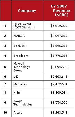 For the record, here are the top 10 global fabless companies of the world, as reported by the Global Semiconductor Alliance (GSA), formerly, Fabless Semiconductor Association, USA.
According to GSA, the total fabless revenue was $27.3 billion, a 12 percent growth year-on-year during 1H 2008. I believe, quite a few, or nearly all of the companies within the GSA top 10 list, have some sort of a presence in India!
Let’s also re-visit the numbers provided by ISA-Frost & Sullivan in its study on the Indian semiconductor industry. The India semiconductor TAM (total available market) revenues will likely grow by 2.5 times, and the TM (total market) will likely double revenues in 2009. Is this not good enough?
Bear in mind that India also plays an active role in the verification and software domains, and it is increasingly covering the entire design chain. The fabs. vs. fabless debate has been going on since 2004-05. Back then, too, many industry observers were backing the fabless route. Now, this discussion is perhaps, a non-issue, with the fabless segment easily the star performer.
India has long had the expertise in chip/board design, embedded software and system engineering. Also, the product and service differentiation is being increasingly driven through software, where India already enjoys a lead over other the APAC countries.
India distinctly has a tremendous opportunity to lead the global market in both semiconductors and electronic products, with or without fabs, or even being fabless!
India leads world in semicon: S. Janakiraman
 Irrespective of the debate raging within the semicon community regarding the IC wafer fabs in India, the strength of and the talent within the Indian semiconductor industry has never ever been in doubt.
Delivering the welcome note at the recently held ISA Technovation 2008 awards ceremony at the Indian Institute of Science, S. Janakiraman, the former Chairman – India Semiconductor Association, and President & CEO – R&D services, MindTree Ltd, elaborated the fact that India now leads the world through execution of most complex and latest technology designs.
Former president of India, Dr. APJ Abdul Kalam was the Chief Guest at the function.
Commenting on the ISA’s role, Janakiraman said that it has been an industry driven body focused on the unique needs and progress of the semiconductor and related industries in India to make it vibrant and project India as a global leader. The ISA’s journey began four years back, in late October 2004, in Bangalore, under the mentorship of Dr. Sridhar Mitta, when like minded industry leaders gathered together and debated how India can achieve leadership position in the semiconductor space similar to IT and software.
Janakiraman said: “We have come a long way since then and today ISA is recognized by everyone in the country and all such bodies outside, as the sole representation of the Indian semiconductor industry. This has been a significant achievement and made possible by all.”
Today, there is a good presence of both Indian and MNC organizations, large as well as start-up companies, design, as well as manufacturing organizations, with the members of ISA now totaling 130! The ISA also works closely with central and state governments to give shape to the aspiration of our industry. It had played a key role in framing the semiconductor policy that enables larger investments in the semiconductor manufacturing ecosystem.
He added: “India has excelled in areas that are knowledge intensive. Semiconductor design is no exception, and today, we lead the world through execution of most complex and latest technology designs. The market size of the IC design and embedded software industry in India was $6 billion in 2007 and has the potential to grow into $43 billion by 2015. It currently employs around 130,000 engineering professionals.”
ISA Technovation Awards
One of the primary charters of the ISA is the talent initiative. This initiative focuses not only on generation of quality talent aligned to the needs of the industry, but also to recognize innovation and research, that further nurtures talent.
The Technovation Awards were created in 2007 to recognize excellence in Academia that has made us what we are today. These awards have been created to honour semiconductor research in India and to create role models in core technology areas.
The award categories are:
1. TechnoVisionary for life time achievement in the semiconductor area
2. TechnoShield for research entity, lab or a department for excellence in a semiconductor domain of interest
3. TechnoMentor for recognizing academician/researcher for contribution in the semiconductor area
4. TechnoInventor for individual excellence in doctoral/masters researchers
This year, ISA has created two special awards for recognizing researchers from Karnataka which have been instituted by VLSI 2007 committee, under two categories:
1. Best Faculty award
2. Best PG student award
The number of nominations went up multifold in this year and an able set of panelists had a tough task of selecting the award winners.
“Given the vibrant scenario of the industry and importance of the event, we have our great leader and visionary Dr. Abdul Kalam with us today evening to recognize the award winners in person'” added Janakiraman.
“Dr. Kalam had been a role model especially for the younger generation – who are the future of this country. Dr. Kalam has been a visionary and a great inspiration for the community present here. It is a great honour for ISA to have Dr. Kalam amongst us.”
The Award Winners @ Technovation 2008
Technovisionary
Juzer M. Vasi, Deputy Director, Indian Institute of Technology, IIT Bombay
TechnoMentor
Bhargab B. Bhattacharya, Professor and Officiating Deputy Director, ISI Calcutta
TechnoShield 2008 (Rolling Shield)
Indian Institute of Technology, Madras — Semiconductor Devices Circuits & Systems Group (SDCS)
TechnoInventors
(Ph. D category)
Debdeep Mukhopadhyay, Indian Institute of Technology, Kharagpur
Thesis : Design and Analysis of Cellular Automata Based Cryptographic Algorithms
BP Harish, Indian Institute of Science, Bangalore
Thesis: Process Variability –aware Performance Modeling in 65 nm CMOS
D. Mahaveer Sathaiya, Indian Institute of Technology, Madras
Thesis: Modeling of Gate Leakage in Aigan/Gan hemts and nitride oxides
(M Tech category)
Rakesh Gnana David J, Indian Institute of Science, Bangalore
Thesis: Adaptive Keeper Design for Dynamic Logic Circuits Using Rate Sensing Technique
Nayan Bhogilal Patel, Indian Institute of Science, Bangalore
Thesis: Performance Enhancement of the Tunnel Field Effect Transistor for Future Low Stand-by Power Applications
Former president of India, Dr. APJ Abdul Kalam, Chief Guest at the function, advised the Indian semiconductor industry to develop tailor-made chips so that electronic equipment could become more cheaper and competitive.
Growing interest in Indian semicon — top 10 most read articles
It is soon going to be a year since the semicon Web site was launched by CIOL. Over the past year, I have noted with delight the growing interest in the Indian semiconductor industry.
Here is a collection of the 10 best articles for my readers. All articles link to those appearing on CIOL.
1. Indian semicon industry: Early steps taken, miles to go!
The Indian semiconductor design industry had a turnover of US $3.2 billion in 2005 with an engineering workforce of around 75,000. It is estimated to reach US $43 billion by 2015 and provide jobs to 780,000 professionals with a CAGR of around 30 percent for this period.
2. Indian semicon special: Increasing brand value for semicon within India
S. Janakiraman, president and CEO –- R&D Services, Mindtree Consulting, and chairman, India Semiconductor Association (ISA), is quite bullish on the advantages of India and the opportunities provided in the Indian semiconductor industry. Here, he speaks on a host of topics, ranging from the outlook for next year, as well as the fab and semiconductor policies, Indian ecosystem, etc.
3. Indian semicon special: Is the timing right for having fabs in India?
It has been some months since the Indian government announced the semiconductor policy. Some fabs are on the way, and lot of CEOs and other industry leaders from leading global semiconductor majors have been visiting India lately.
4. Indian fab guidelines promise exciting times for semicon, electronics
India seeks investments in ecosystem units for LCDs, OLEDs, PDPs, solar cells, photovoltaics, storage devices, advanced micro and nanotech products, etc.
5. Indian semicon policy ground breaking
These comments from Michael R. Splinter, president and CEO, Applied Materials, were enough to indicate how much the Indian semiconductor policy, announced recently by the government of India, has caught the attention of the global semicon majors.
6. Indian ecosystem will not enable faster product development cycles
The economy of scale may also not justify having a wafer fab facility to cater only to the Indian market, says Dr. H.V. Ananda, Synplicity.
7. India should be known for its semicon might
The semiconductor industry is poised for high growth and will make all round progress be in design or manufacturing or consumption. Issues to tackle are the rising costs and not yet conducive infrastructure.
8. ISA-F&S: India growing almost thrice as faster as global semicon
According to India Semiconductor Association (ISA) and Frost & Sullivan (ISA-F&S), India’s 2007 annual growth in semiconductor market is nearly triple the rate at which the global semiconductor market is expanding.
9. India ascends in the embedded value chain
Indian semicon, embedded design industry to grow from $3.25bn in 2005 to $14.42bn in 2010 and $43.07bn in 2015.
10. India rapidly becoming hub for embedded designs worldwide
India design services companies are involved in embedded hardware and software design in the latest embedded market segments such as automotive infotainment, digital security and surveillance.
I’d like to say a very big thanks to all of my readers. I am also working on another semicon special, which should be out next month on CIOL. The semicon special for 2008 — a collection of industry leading articles, will be online middle of next month.
India's growing might in global semicon
It is no longer a secret that India is fast becoming the world’s destination, and increasingly the source too, for semiconductors. India also shows the most rapid growth potential among the BRIC countries.
Speaking at the recently held International Electronics Forum (IEF) 2008 at Dubai, organized by Future Horizons, S.Janakiraman, the outgoing Chairman – India Semiconductor Association, and President & CEO – R&D services, MindTree Ltd, touched upon India’s growing might as a being the third largest country in terms of purchasing power parity, as well as its growing presence in the global semiconductor industry.
It is no surprise that the current market drivers in India happen to be mobile phone services, IT services/BPO, automobiles and IT hardware. Add to these are the facts that India is very strong in design tools, system architecture and VLSI design, has quite strong IP protection laws, and is quite strong in concept/innovation as far as the semiconductor industry is concerned.
Testing and packaging are in the nascent stage. While India lacks a semicon wafer fab, as of now, there have been several announcements regarding solar fabs by leading firms such as Videocon, Moser Baer, Reliance, etc.
In the electronics manufacturing domain, India’s strength lies in hardware, embedded software and industrial design, OEMs, component distribution (includes semiconductor and box build), and end user/distribution channel, as well as more than moderate strength in product design and manufacturing (ODM, EMS).
India is likely to witness $363 billion of equipment consumption and $155 billion of domestic production by 2015. India’s electronic equipment consumption in 2005 was 1.8 percent. It is likely to grow to 5.5 percent in 2010 and 11 percent in 2015, as per a joint study conducted by the ISA and Frost & Sullivan.
The Indian semiconductor TAM (total available market) revenue is likely to grow by 2.5 times while the TM (total market) is likely to double revenues in 2009. The TAM is likely to grow at a CAGR of 35.8 percent and the TM is likely to grow at a CAGR of 26.7 percent, respectively, during the period 2006-09.
Telecom, and IT and office automation are currently the leading segments in both TM and TAM. Consumer segment occupies the third fastest growing area in the TM, while the industrial segment is the third fastest growing area in the TAM.
The major semiconductor categories include microprocessors, analog, memory, discrete and ASIC, while the major end use products include mobile handsets, BTS, desktops, notebooks, set-top boxes and CRT TVs.
Emerging base of EMS firms
India is also becoming an emerging base of EMS companies, thereby completing the electronics ecosystem. Five of the top 15 EMS companies globally have set up their manufacturing facilities in India. These include Celestica, Elcoteq, Flextronics, Jabil Circuit and Solectron. Two other large companies are in the process of setting up plants — Hon Hai Precision Industry and Sanmina-SCI.
Nokia has set up its manufacturing facility as well. It has invested $210 million in the plant since January 2006. The India plant has set another benchmark of achieving the fastest ramp up across all Nokia facilities worldwide. Currently, approximately 50 percent of the production from the plant is consumed domestically and the rest is exported to other countries.
Indian embedded design industry
The Indian embedded design industry has been going from strength to strength. The recent IDC-ISA report puts revenues from India’s VLSI, board design and embedded software industry to grow to $10.96bn by 2010 from the current $6.08bn in 2007.
As of 2007, embedded has 81.1 percent share, hardware board design 6.3 percent; and VLSI design 12.3 percent, respectively.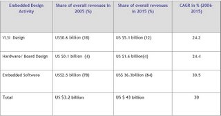 Source: ISA.
The challenges and focus areas for the embedded design industry include manpower — focusing on increasing productivity, creating readily deployable engineering workforce, and focusing on developing high-end skills.
Another area India is working on is moving up the semiconductor value chain. India is now focusing on end-to-end product development, investing in IP development, developing India specific products, and partnering with OEMs to understand the market needs.
The challenge is posed by the cost structure. India needs to better address cost management, i.e., increasing infrastructure and salary costs, as well as managing the dollar’s impact.
India design inside
Several global products have been now developed out of India. Some recent examples are: Harita Infoserve Ltd is developing interior parts and conducting computer tests on components for General Motors Corp.
Next, Ittiam’s videophone design will become almost entirely an India story: part of the chip, the product design, the software and, finally, the manufacturing also done here. Plexion Technologies has worked on the interior design and windows for a DaimlerChrysler (DCX) bus.
Quasar Innovations designed and developed a dual SIM card — PTL910 mobile phone for Primus, to be launched in the European market. The mobile phone allows the user to have SIM cards from Primus for two countries, with the phone automatically choosing the correct SIM depending on the user’s location.
Finally, MindTree itself has designed a feature rich satellite handset with mobile handset form factor for a European company.
Attractive semicon policy
India’s semiconductor policy is likely to attract investments of over $10bn. The government of India will bear 20 percent of the capital expenditure during the first 10 years for units located inside SEZs and 25 percent for those outside.
For semiconductor manufacturing (wafer fabs) plants, the policy proposes a minimum investment of $625mn. The same for ancillary plants would be $250mn.
The government’s participation in the projects would be limited to 26 percent of the equity portion. The key benefit here is the grant of the SEZ status.
India’s evolving ecosystem is driven by the bottom of the pyramid (BOP) opportunity. Tata Motors announced the now famous Nano — the Rs. 1 lakh (sub $2500) car -– said to be the world’s cheapest car. This has been indigenously developed in India, for India, by Tata Motors.
Nano has passed all mandatory crash tests and Euro IV norms. It is likely to be commercially launched in the second half of 2008.
All of these make India the most happening semiconductor and electronics destination. Don’t be surprised if companies not having an India strategy in place miss out on the action!
