Archive
ISA, UK-TI MoU to develop semicon industry
 Recently, the India Semiconductor Association (ISA) signed an MoU with East of England International (EOEI) to promote and develop the semiconductor industries in their respective domains.
On August 31st, which is early next week, the ISA and the UK-TI will be signing an MoU to extend this relationship further.
My colleague, Usha Prasad and I met up with Chandrika Anil, Manager – Membership Services, ISA, to hear more about the MoU.
Elaborating on how the MoU between the ISA and UK Trade & Investment (UK-TI) is going to help in encouragement and development of Global Value Chain Partnerships, Chandrika said that the ISA and the UK-TI share a mutual interest to promote and develop the sector semiconductor industries in their respective domains. The MoU between ISA and UK-TI entails promotion of the concept of Global Value Chain Partnerships.
As part of the MoU, the two organisations have agreed that:
- Global Value Chain Partnerships are of mutual benefit in the ongoing development of the Indian and UK semiconductor industries and the relationship between them.
- ISA and UK-TI will co-operate with each other in the following activities to encourage and develop Global Value Chain. Partnerships between Indian and UK semiconductor firms. This allows for:
- Promoting the concept of Global Value Chain Partnerships amongst the Indian and UK semiconductor industries in the most appropriate manner
- This may include website, newsletters, conferences and direct discussion with firms.
- Identifying, through ongoing research and discussion, areas of potential business opportunity which could be addressed by Indian and UK firms working together
- These areas could form a set of themes around which ISA and UK-TI may wish to focus on seminars and other activities to raise awareness, understanding and interest.
- Encouraging firms in the two industries to register (free of charge) their interest in exploring relevant partnerships and business opportunities in the identified areas
- This would involve inviting firms to provide information about their interests and capabilities, periodically reviewing identified opportunities which may be relevant
- Facilitating meetings between firms and groups of firms to take forward discussions with a view to formation of Global Value Chain Partnerships
The MOU will create a synergy between India and the UK in the areas of design, device and applications.
You can read more on ISA’s website. Thanks for the interaction, Chandrika, and well done, Usha!
Top trends for global/Indian semiconductor industry in 2009
Right then, folks! Here are the much awaited top trends for global semiconductor industry for 2009!
First, let’s start with microprocessors and microcontrollers. One of the most apt persons to answer this query was Jordan Plofsky, senior vice president, Market, Altera Corp., during his recent visit to India for the Altera SOPC Conference.
Top trend in microprocessors/microcontrollers
Undoubtedly, the major trend will be the shift to multicore and its challenges. These challenges include:
* Parallel programming tools.
* Memory bandwidth allocation.
* O/S support.
* Verification tools.
* Power reduction and performance improvements.
In one of my previous blogs, I had discussed with Intel how parallel programming is getting to be regular! Also, AMD is well on an identical path! Hence, this key global trend is very much in line with the focus on parallelism!
Top global semiconductor trends for 2009
According to Plofsky, the major trends would be:
* Consolidation
* Power management
* Supply chain dynamics changing – inventory reduction
* Focus on operational costs in a slower growth environment
Indian semicon trends
And what about the top trends for the Indian semiconductor industry? Here are some thoughts from S. Janakiraman, former chairman, India Semiconductor Association (ISA) and President and CEO-R&D Services, MindTree.
Top 5 trends for Indian semicon industry in 2009
According to Jani Sir, the key trends in India during 2009 are:
* Global customers will have higher cost pressure and increase level of offshoring and outsourcing in 2009.
* India will become an even more important market for selling semiconductors as India will show higher percentage growth than other markets.
* Decided in India and originated in India products will licensed and manufactured for the global market.
* Business models for design services will start shifting from T&M and linear with people strength to risk-reward, non linear and more skin in the game.
* India will start inventing products that matter to rural and bottom of the pyramid segments.
All of these are in line with what’s happening in the Indian semiconductor industry — focus on embedded and design services, coupled with product development, which is beginning to see several starts. Also, several MNCs are now designing products out of India. Two recent top-of-the-mind instances are those of Intel and AMD. Others will follow suit, definitely.
Well, these trends could be tough to beat! What do you think folks?
Four key drivers for Agilent!
Agilent has been a leader in T&M for quite some time, and India remains a key market for the company.
According to Venkatesh Valluri, President and Country General Manager, Agilent Technologies India, the global market size for T&M in electronics and life sciences is $43 billion. This includes $18 billion in electronics and $25 billion in life sciences. From the India side, the size is about $1 billion.
He says: “Testing is becoming a more integral part of the product development process, especially in general electronics. It is now coming of age. As for the rate of expansion, it is approximately 15-20 percent YoY, and it is higher in India than in other parts of the world.”
Drivers for T&M
Telecom has been the leading driver. However, telecom growth may not be sustained YoY, for say, the next 10 years. “You can’t get 100 million subscribers each year! The difference would be more in the quality of service (QoS). This automatically drives testing and measurement,” he adds.
The second driver is the aerospace industry. The difference is through high-end technology. Agilent’s ADC conversion technology is one of the best in the world. In the next few years, new programs will make this segment even more stronger.
The third driver is manufacturing electronics. In India, it is definitely not as aggressive as China, but it is coming up. Even most of the EMS players are present here. Therefore, some ecosystem is building up.
The fourth driver is the design validation process. As the global R&D centers start coming into India, the companies are also starting to do product design.
Agilent in solar
Hold it guys! Agilent is all set to play a big role in the emerging solar/PV segment as well. According to Valluri, in India, solar/PV is getting into a manufacturing transition.
He notes “Agilent plays strongly in the nanomeasurement area. As solar emerges in India, nanomeasurement technology will become important. Agilent has the AFM (atomic force microscopy), which is a leading product line.”
Semicon in India
All of the large semiconductor companies are based in India. Also, a lot of high-end work is also happening here. The design validation market is slowly coming up.
Agilent feels that the semiconductor companies would need products with the right price points. There will be a need to build the right value at the right price points, says Valluri.
On the gloomy economic climate, he agrees that while the economic climate will not be so robust in 2009, Agilent operate in markets that are considered steady. “We believe that it will be reasonably okay to remain committed to such markets,” he says.
China, India largest growth markets
Ron Nersesian, Vice President and General Manager, Wireless Business Unit, Electronic Measurements Group, Agilent, points out that it is good to see growth that has been happening.
He says: “Growth in our business has been exceptional. It is an opportunity to work with the local companies as well as the Nokias of the world. We also see opportunities in aerospace and defence, wireless R&D, and installation and maintenance areas. China and India are the largest growth markets.”
Agilent’s strategic intent is to become the leading test and measurement company.
“If you look at the new wireless standards, we would like to provide solutions for all of these standards. We are working on both WiMAX and LTE. We are working with the top wireless vendors as well, says Nersesian.
In aerospace, Agilent work on signal analyzers, signal sources, etc. It also makes network analyzers and component test products, as well as non-linear vector analyzers.
Agilent has also invested in the network surveillance area. “We are focusing on RF surveillance and solutions as well, which can be of great interest to the Indian government,” adds Nersesian.
No fabs? So?? Fabless India shines brightly!!
This is no secret: fabs or no fabs, fabless India has been shining brightly all this while and will continue to do so for some time!
I’ve blogged on numerous occasions about India’s strength in design services, India as the embedded superstar, and well, about India’s growing might in global semicon. A fab will surely boost India’s image on the global map, but it is definitely not that essential!
It was very pleasing to hear S. Janakiraman, former chairman, India Semiconductor Association, and President and CEO-R&D Services, MindTree, also highlight this fact at Altera’s SOPC conference recently. Perhaps, India has been emphasizing on having a fab. However, if the fabless segment keeps growing as it has been up until now, that would boost industry growth as well!
Top 10 global fabless companies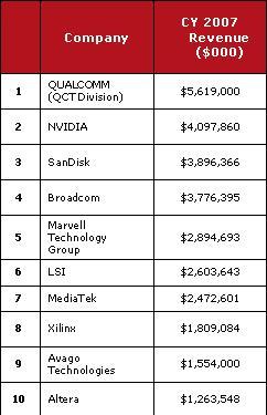 For the record, here are the top 10 global fabless companies of the world, as reported by the Global Semiconductor Alliance (GSA), formerly, Fabless Semiconductor Association, USA.
According to GSA, the total fabless revenue was $27.3 billion, a 12 percent growth year-on-year during 1H 2008. I believe, quite a few, or nearly all of the companies within the GSA top 10 list, have some sort of a presence in India!
Let’s also re-visit the numbers provided by ISA-Frost & Sullivan in its study on the Indian semiconductor industry. The India semiconductor TAM (total available market) revenues will likely grow by 2.5 times, and the TM (total market) will likely double revenues in 2009. Is this not good enough?
Bear in mind that India also plays an active role in the verification and software domains, and it is increasingly covering the entire design chain. The fabs. vs. fabless debate has been going on since 2004-05. Back then, too, many industry observers were backing the fabless route. Now, this discussion is perhaps, a non-issue, with the fabless segment easily the star performer.
India has long had the expertise in chip/board design, embedded software and system engineering. Also, the product and service differentiation is being increasingly driven through software, where India already enjoys a lead over other the APAC countries.
India distinctly has a tremendous opportunity to lead the global market in both semiconductors and electronic products, with or without fabs, or even being fabless!
Synopsys' Dr Chi-Foon Chan on India, low power design and solar
There have been reports about the troubles within the EDA industry in recent times, especially those related with quarter sales. Interestingly, Synopsys has been the one sailing along fine! If that’s not enough, it made its intention known of playing a role on the solar/PV segment, an area where lot of investments have been happening!
 Given this scenario, I was fortuitous enough, rather, extremely lucky to be able to get into a conversation with Dr. Chi-Foon Chan, President and Chief Operating Officer, Synopsys Inc., during his recent visit to India.
On the state of the global semiconductor industry, he said, it was somewhere now in the low 10s [well below 10 percent]. The EDA industry is currently tracking below that level. However, Synopsys has been growing at around 10 percent. He said, “The technology challenges today are very high.”
Synopsys has a substantial number of R&D population based out of India. Giving his assessment of the Indian semiconductor industry, Dr. Chan added: “Our main interest in India is largely talent and the academia. India can very well get more into the product development side. Even the outsourcing of designs have increased. Our capabilities, of the Indian team, have also increased.”
As with any good semiconductor ecosystem, the Indian industry also needs a proactive industry association, a role played to near perfection by the ISA (India Semiconductor Association). Acknowledging the ISA’s role, Dr. Chan said, “The ISA has also formed a very cohesive team.”
There is little doubt about India’s growing importance in technology strengths and managerial leadership. Dr. Chan added: “We are more on the high-end side and also track what others design. In India, the profiles of designs are definitely high-end in nature. This is largely due to the presence of a large number of MNCs. A very high percentage of designs are in the 45nm and 65nm process technology nodes.”
There is another significant indicator of India’s growing importance, and that is the huge rise in the attendance of the SNUG. In 2000, this event attracted 180 people. However, in 2008, the SNUG attracted over 2,000 people.
Moving India to next level
Given the very high level of commitment on Synopsys’ part toward India, there was a need to find out from Dr. Chan what exactly India needs to do to move to the next level in the value chain in the semiconductor ecosystem.
He advised: “India can do two to three things. One, for the system to grow, you need the government, academia and industry to grow together. India has all of the ingredients required to drive products.”
Comparing India with China, he highlighted the fact that while in China, the local consumption was higher than local supply, that was not the case with India!
“Therefore, looking at merely the local market is not the only thing. Products developed here can also be targeted at the Middle East and Southeast Asia.” He was quite forthright in his analysis, adding: “Industries start when you find markets. The skill sets are already present here. There can well be multiple startups.”
Dr. Chan also touched upon the fab vs. fabless issue, noting that there could well be more of fabless companies in India. “Building a fab requires lot of capital. Also, consolidation will continue to happen.”
What role does Dr. Chan see Synopsys playing in the Indian context? He said: “Synopsys will continue to be a catalyst for the industry. A healthy design industry in India continues to help us. We also work well with the Indian universities. Having more people from the universities will always help. We also invest a lot in application support. The application team also trains others. I now look forward to seeing more fabless companies here and India to become even more global.”
On low power design
India is also a centre of expertise in low power design, given that low power is hugely important in today’s electronics ecosystem. Dr. Chan commented that low power has always been the number one design issue. It cannot be taken care of at one single stage.
He added: “A slightly new concept that has emerged is low-power verification. There are so many schemes for attacking low power, such as multiple voltage islands. We (Synopsys) are spending a lot of effort in low power.
“As a designer, you require detailed analysis. Low-power verification is now coming up. Another area is testing. As an example, if so much power is required, how do you have the power cut from the tool you are using to test? From a Synopsys point of view, we are involved in several points, such as front-end synthesis, testing, sign-off, verification, etc. We are trying to put in a whole lot of methodologies.”
Synopsys in solar
EDA may be able to help by lowering power requirements and leakage on better products. Especially, the Synopsys’ TCAD product can be used to create more efficient and effective solar cells. Now, this is not a new development anymore. Synopsys, along with Magma, have already made known their intentions about setting foot in the solar/PV space.
On the TCAD, Dr. Chan said: “We have a very strong position in the TCAD, commercially. Now, it is one of our most critical elements in high-performance. Our TCAD is among the strongest in the EDA industry.
“In solar, it does not have to be a complicated place-and-route, etc. From an entire solar industry point of view, we have now used some effort from TCAD into this space. Heat transfer issues, etc., are more in the EDA space.”
I will continue my conversation with Synopsys on its solar initiative sometime later. Keep watching this space, folks
Practical to take solar/PV route: Dr. Atre, Applied
 Solar/PV is perhaps, a practical route for India to enter manufacturing, contends Dr. Madhusudan V. Atre, president, Applied Materials India. Alternatively, another way to enter this field could be by having solar farms.
According to Dr. Atre, India has a strong potential for manufacturing. The Indian scenario has the talent pool and an emerging middle class, along with the presence of system design and chip design companies. Only a fab seems to be the missing piece from this ecosystem!
Benefits of a fab include: fuels economic productivity, contributes to GDP and adds to national growth, creates jobs, helps set up the other expertise necessary for an ecosystem, and closes the loop between market, design, manufacture, test, customer.
Indian fab scenario
Commenting on the Indian scenario, Dr. Atre, says: “For PV, about $200-500mn is needed for a fab. If we can enter into manufacturing via the solar/PV route, the scale of investment required would be much less [than the investment needed for a wafer IC fab]. This can be practical route to enter manufacturing in India, and less complexity is involved, as compared to an IC fab.” Another way of entering manufacturing is by having solar farms.
Applied’s external face in India involves: Take leadership role in industry bodies; work with the government on various semiconductor and manufacturing policies; look for potential investments in start-ups; work with the academia on collaborative research in nanomanufacturing; be sponsors in key conferences; drive corporate social responsibility programs; and help enable semiconductor and solar manufacturing in India.
Touching on some emerging areas of interest, Dr. Atre highlights that packaging is very important in semiconductors. “We may look at some company in packaging R&D. We have invested a bit in Tessolve,” he says. “We would also like to see the success of the nanotech lab in IIT-Mumbai, and see how it can help India.” On a global scale, he notes that Applied would be setting up two-three SunFab lines with Masdar in Abu Dhabi, UAE.
Applied Materials in India
Headquartered in Bangalore, Applied has been present in the country for over five years. It has approximately 1,500 employees and associates. A liaison office was originally set up in May 2002. Applied Materials India Pvt Ltd (AMIPL) was set up in July 2003, and operations started in November 2003 with cost + model. It consolidated all Applied operations in Bangalore into ITPL (~92,000sqft). It also merged Brooks Chennai (~100RFTs) into Applied India operations. Applied currently has R&D centers in Bangalore and Chennai.
Next, Applied established site operations in Delhi (~5000 sqft) to support Moser Baer. Its key partners are Satyam, Wipro and TCS, on various aspects of engineering and software services. In Delhi, Applied has 25-30 people to support Moser Baer, where it has the first SunFab line up and running.
In Mumbai, it has set up a nanomanufacturing lab with IIT-Mumbai. “We have put in equipment worth $7-8 million there, and do R&D projects,” adds Dr. Atre. The nano lab at IIT-Mumbai was inaugurated in November 2007 by Mike Splinter, president and CEO, Applied Materials.
Applied is also involved in the potential upgrade of SCL. “We are working with some other companies on how we can upgrade SCL. We are more at the backend to set up some capabilities,” he says.
Applied Ventures makes investment in emerging technologies and companies. It has funded a couple of companies in the semi start-up stage. Applied Ventures looks at global investments.
Moser Baer is Applied’s first customer in India. It has a 35-40MW assembly line. This is the first time that 5+m2 solar panels will be coming out. The panel will now have to be taken up to the production ramp. Dr. Atre adds that Europe was much advanced in solar/PV. Germany, especially, was far advanced in the implementation aspect, as well as Italy and Spain.
Nanomanufacturing simplified
Nannomanufacturing, as per Wikipedia, is “the near-term industrial-scale manufacture of nanotechnology-based objects, with emphasis on low cost and reliability.” To manufacture at this level requires a lot of expertise, skills, etc., says Dr. Atre. Cost is definitely an important driver, and so is reliability, he adds. According to him, nanomanufacturing technology combines the two core strengths of Applied: nano + manufacturing.
Applied’s vision has been to apply nanomanufacturing technology to improve the way people live. Its mission: To lead the Nanomanufacturing technology revolution with innovations that transform markets, create opportunities, and offer a cleaner, brighter future to people around the world.
Applied Materials is a global leader in nanomanufacturing technology solutions with a broad portfolio of innovative equipment, service and software products for fabrication of: semiconductor chips, flat panel displays (using TFTs), solar photovoltaic cells and modules (in crystalline and thin film vectors), flexible electronics, and energy efficient glass (BIPV). The last three categories fall under EE or the Environment and Energy Division.
Dr. Atre says: “We have the SunFab line for solar/PV. In flexible electronics, as an example, you can have solar cells wrapped around an object.” As for energy-efficient glass, you can save on AC costs, etc., by using building integrated photovoltaics.
Core capabilities
Applied’s core capabilities include: commercialize sophisticated systems and thin-film engineering, besides a global culture. “Our technological strengths include semiconductors, solar/PV cells and FPDs. We have nanomanufacturing technology as the common theme.” Touching on the loss per watt, he says it is currently around $14, which needs to come down to at least $2 or one-fourth.
Applied makes systems used to produce virtually every new microchip in the world, taking care of thermal, etching, inspection, PVD, CVD and CMP. For LCD flat panel display systems, Applied offers a variety of systems, such as PECVD systems, e-beam array testers, PVD systems and color filter sputtering systems.
The processing panels can be up to 2.2×2.5 meters. For solar manufacturing, Applied offers crystalline silicon, flexible PV and thin-film line, or the Applied SunFab lines. For architectural glass and flexible electronics, it offers both glass and Web coating systems.
“We have three key businesses, silicon systems, displays and energy and environmental solutions,” said Dr. Atre. These are supported by Applied Global Services.
Applied’s goals for 2010 include: Expanded revenue streams, to become a $13-15 billion company; increased operating efficiency, with margins >25 percent, and increased cash flow, about >20 percent of revenue.
Premature to write off Indian fab story: Dr. Pradip Dutta
The previous blog was focusing on SemIndia and the notice it has received on the Fab City in Hyderabad, along with NanoTech. BV Naidu, a friend and an industry colleague, has put up a strong front, and is trying his best to ensure things get going in the IC wafer fab space in India. Best of luck to him and SemIndia. India needs a fab, much more than ever, now.
 I also happened to have a brief chat with Dr. Pradip K. Dutta, Corporate Vice President & Managing Director, Synopsys (India) Pvt Ltd, another friend and an industry colleague. Although from the EDA industry, Dr. Dutta has great thoughts and ideas regarding the future of semiconductors in India.
According to him, building wafer fabs in India involves an element of national pride and should also make business sense, simultaneously. The government has to look at fabs from a national policy perspective. If there were any company breaking ground in India, to build a clean-room, we would have known, he states, which is very correct.
We all know that a fab is a highly capital intensive project. He says: “I hope we can see some concrete proposals by this time next year. It is too premature to say that the Indian fab story is disappearing.”
There is a need to bear in mind that fabs in India have a three-year window. So, there is no reason for getting worked up right now, as the window is still there and existing. Dr. Dutta adds: “The business people will only open up their cards in the final stages. I have reasons to believe by summer of 2009, there will be some actual stakeholders.”
A fab is a very economically complex business. In the next five-10 yrs, there is a strong feeling that there may be only three to four companies globally, as IDMs, and the rest move into foundry. Dr. Dutta stresses: “To expect India will have a 5bn, 45nm, capable fab is something that needs to be examined. The business case has to be the driver.”
The semicon policy has definitely been a good start. What has since happened since that the ancillary manufacturing industry has been taking advantage of the policy.
“The government is quite optimistic that as we reach next year, by this time, companies will firm up their plans, as the industry window is three years. We believe that concrete proposals will come in by that time,” reiterates Dr. Dutta.
The government wants to see a state-of-the-art facility come up as well. He notes: “Maybe, 50 percent of all ICs sold globally, can be built on 0.25-micron technology. However, under the current semicon policy, we want to encourage state-of-the art manufacturing.”
Given the current global economic scenario, it will take real effort on part of all the stakeholders and come up with a wafer IC fab. India seriously needs a fab! There’s a huge market out there, which needs to be tapped. Delays will only add to our slipping back.
Indian semicon needs concrete plans
 The Indian semiconductor market is still in a nascent stage. In the Indian context, while we are very good in design services, we have yet to achieve the required capability to build products.
In this context, Subhash Bal, Country Director, Synopsys (India) EDA Software Pvt. Ltd says: “One has to first understand the dynamics of the semiconductor market. The key is: if you grow a market here, it will also grow somewhere else. That’s where the trick lies!”
The Indian semiconductor industry really needs to figure out what will work! “It would be better to think about solving a particular problem, which will go on to solve a bigger problem for India. There is also a need to build incentives to go along with al of this,” adds Bal.
He states: “We should produce a plan to take semiconductors forward in India. We need to be realistic about what we can do with the semiconductor industry. India should better be up there, at the top, in terms of technology as well. For example, RFID can be used in a whole range of applications.”
Way forward
What can be the way forward for the Indian semiconductor industry? First, there is a need to create a plan for Indians residing in the USA to return home and start something. They should be offered a lot of incentives as well. Next, there is a need to allow developing schemes where Indian applications become the focus, especially for high-volume government applications, such as traffic light controls, ID cards, toll tax applications, etc.
“Such things will only trigger demand. It will also see the rise of Indian product companies, and later, those will grow into semiconductor companies,” advises Bal.
Indian fab story disappearing?
Is the Indian fab story disappearing from sight? Not exactly! There will be a lot of solar fabs coming up, while it is still early days for wafer IC fabs. Fabs for PV cells are relatively easy to set up. Undoubtedly, PV has a huge market potential.
On the subject of fabs, Bal says: “The technique of management of fab technology is crucial. There should be some government schemes for smaller fabs as well. It does not matter whether these are 150mm or 180mm fabs. Indigenous applications can source simple applications, such as autorickshaw meters, toll tax applications, etc.”
Bal, like many others, believes that the next decade clearly depends on the youth of India. Therefore, this plan for semiconductors has to be long term — for about 25-30 years — and action oriented. This has to start from an end solution, and thereafter, semiconductors should be able to take off!
“Apart from such a plan, it is also important that sufficient attention is given to developing the right infrastructure. Infrastructure needs to be fixed as well. Should these be addressed, the semiconductor industry in India will likely take off,” adds Bal.
Globally, Synopsys has been growing steadily. In fact, the Q1-08 revenue is likely to close at $325 million. Synopsys India has a current headcount of over 600 employees, located in Bangalore, Hyderabad and Noida. The activities of the Hyderabad center is global in nature.
Top semicon articles of 2008
A very kind reader left a comment yesterday that he (or she?) spent three hours on my blog! I am simply overwhelmed and humbled!!
It has really been a pleasure writing and maintaining a semicon blog! Plenty such are around carrying very valuable information, and I salute those bloggers.
It is really tough to contend with all the other technology-related information, but then, semicon has its own charm, and its own set of dedicated readers — who DO go on to become extremely loyal.
I am even more touched by another request by a friend to list all the top articles I’ve written this year. Wow!!
It is very difficult for me to say, which ones are the best! However, I am listing the articles here. They all link back to CIOL. Of course, I’ve blogged here first, so, those who are familiar with my blog pieces, will identify them immediately.
Here goes then — starting from the latest back down to very late last year — in terms of relevance. Enjoy!
Semi trends 2008: Fab spend lower, ASPs stabilizing
The call on global fab spend was for a 10 percent reduction, and this is now getting to be closer to 20 percent.
UK, India aim for semicon collaboration
ISA-UKTI study examines collaboration scope between India and UK in design, applications and devices.
Dubai an emerging silicon frontier
The government of Dubai has set up the Dubai Silicon Oasis Authority (DSOA) as the engine for propelling Dubai into the knowledge economy.
Be parallel, or perish!
Parallelism offers new doors, and creativity is required to open these new doors, says Intel.
Altera first @ 40nm FPGAs
The company has announced two product lines — the Stratix IV FPGAs and the HardCopy IV ASICs.
Semicon likely to grow 12pc in 2008
If there will be an economic recession, the chip industry (but not all firms) is in the best shape possible to weather the ensuing storm.
India’s growing might in global semicon
India is fast becoming the world’s destination, and increasingly the source too, for semiconductors.
Fascinating developments in 22nm!
These augur well for the global semiconductor industry, even though the field could get much narrower.
Indian design services to touch $10.96bn by 2010
Total design services market in India is said to have grown at 21 percent year on year.
NXP India achieves RF CMOS in single chip
The entire analog and RF work done has been in Bangalore by NXP’s single-chip design team.
LabVIEW 8.5 delivers power of multicore processors
With LabVIEW, designers and engineers can assign different tasks on different cores — which are independent.
Multi-nationalization of product development process
Indian designers lead in transaction level design, and can play big role in EDA.
Can we expect exciting times in 2008? Some trends
Blurring lines between PMPs and PNDs, semicon rush or hush; Netscape’s end — all are in store!
Semicon outlook 2008: Global market likely to grow 6-11 percent in 2008
Some predictions are for 2008 to be flat year or a year of negative growth; EDA to grow 7.8pc!
That’s about it! If there’s anything I’ve missed out, kindly let me know. Thanks for all your continuing support, dear readers. It is very humbling and touching.
