Archive
Renesas Mobile inaugurates R&D centre in Bangalore
Renesas Mobile Corp., a wholly-owned subsidiary of Renesas Electronics Corp., announced the inauguration of its research and development (R&D) centre in Bangalore, India which develops 2G, 3G and 4G modem technologies.
: Heikki Tenhunen, senior VP, Alan Frederiksen, MD, Renesas Mobile India, Shinichi Yoshioka, senior executive VP and COO, and Jean-Marie Rolland, CTO and executive VP, Sales and Marketing.")
(L-R): Heikki Tenhunen, senior VP, Alan Frederiksen, MD, Renesas Mobile India, Shinichi Yoshioka, senior executive VP and COO, and Jean-Marie Rolland, CTO and executive VP, Sales and Marketing.
Renesas Mobile was established on December 1, 2010 as a 100 percent subsidiary company of Renesas Electronics. As part of the Renesas group, it has the support of the world’s largest embedded microcontroller player in the semiconductor world. Renesas Mobile focuses on platforms for smart phones, feature phones, car infotainment and embedded connected devices enabling people to stay connected in the cloud computing era.
The company integrates the former Mobile Multimedia Business Unit of Renesas with the former Nokia Wireless Modem Business Unit. The Nokia Wireless Modem Business Unit has been acquired by Renesas Electronics as announced on July 1st, 2010.
Introducing Renesas Mobile Corp., Heikki Tenhunen, senior VP, said that Renesas Mobile offers advanced and innovative products and services for mobile phones, car infotainment solutions, consumer electronics and industrial applications.
The company’s mission is to develop, productize and deliver advanced triple- and dual-mode communication centric semicon chipsets and platforms based on chipsets to provide innovative solutions and drive mew oppurtunities for customers. Renesas Mobile aims to be a world leader in mobile platforms by evolving its proven modem, application processor and SoCs, and associated services via its global business channel.
The Renesas-Nokia combine has since gone on to make unrivalled connected experiences a reality — by way of powerful multi-tasking, rich multimedia, newly emerging technologies — such as cloud computing, 3D, augmented reality, etc., PC like Internet experience, smaller form factor and longer battery life, and remain always connected!
Renesas’ mobile expertise includes the following:
* Excellent device experience, supporting over 400 mobile handsets to date;
* Key components verified at ‘system‘ level quality for platform release;
* Complete reference design easy to start application development;
* Market proven multimedia software package and multiple OpenOS integration support;
* Competitive SoC implementation performance; over 470 mn transistors in mobile LSI (G4);
* Leading-edge process (45nm, 28nm, 22nm) balancing own fab and partners (TSMC, etc.). Read more…
New apps in semicon — smart grid and secure transactions
Happy new year and welcome to my blog.
Let’s start this year by looking at René Penning de Vries, senior VP and CTO of NXP, who spoke this morning at ISA’s CXO Conclave, titled New Applications in Semiconductors (Smart Grid & Secure Transactions) – Role semiconductors play to make our society a better place!
Dr. René Penning de Vries touched upon the role semiconductors play in two of the societal mega-trends: energy and security. In 21st century, IC industry has gone from business driven to society driven and semiconductors play key role in solving problems like energy shortage and security threat. In essence, semiconductors make our lives better.
The first part of this talk touched upon “smart grid”, it’s applications, and associated semiconductor innovations in AMS domain. The second part covered “secure transactions”, innovation, and transition in this domain from “IC hardware focus” to “HW-OS-Apps holistic”. Rene illustrated with real-life NFC example from the recent Google-NXP collaboration.
According to Rene, the IC industry is being driven from business to consumer, and now, to society. Some of the well known areas where ICs are being used today include health and wellness, transport and mobility, security and safety, energy and environment, communication and e-society.
Some of the key macro drivers in electronics include:
Energy efficiency: Includes efficient power conversion and low stand-by power, energy-saving lighting and back-lighting, energy conservation through demand side management, electric/lighter vehicles, and intelligent traffic management.
Connected mobile devices: Includes proliferation of mobile data usage, wireless infra build-out, smart mobile devices: always-on, multimedia, location-based, connected car, many broadcast and connectivity standards, and new user interfaces (e.g., touch, joystick).
Security: Includes secure mobile transactions and secure identity, authentication, tagging and tracking, car and home access, security and remote diagnostics, and radar and (body) scanning installations.
Health: Includes personal healthcare and portable emergency devices, connected hearing aids and implantable devices, car safety and comfort, and electronic diagnostics.
Key application areas include:
Wireless infrastructure: Wireless base stations, satellite, CATV infrastructure and radar.
Lighting: Lighting, LED, backlightingIndustrial: Smart metering, white goods and home appliances, Pachinko, medical, industrial and ATE.
Mobile: Mobile handset, portable power supplies and hearing aids.Automotive: Car access and immobilizers, in vehicle networking, car entertainment, telematics, ABS, transmission and throttle control, and lighting.
Identification: Secure identity, secure transactions, tagging and authentication.Consumerr: TV, satellite, cable, terrestrial and IP set-top boxes, and satellite outdoor units.
Computing: Monitor, power supplies, personal computer TV. Read more…
Qualcomm, AMD head top 25 fabless IC suppliers for 2009; Taiwan firms finish strong!

Top 25 fabless IC suppliers for 2009. Source: IC Insights
So, IC Insights has revealed the top 25 list of fabless IC suppliers for 2009! No surprises, Qualcomm still leads!
However, AMD is the surprise runner-up, for now. The reason being: AMD became a fabless company by including its Dresden, Germany fabs as part of GlobalFoundries spin-off. IC Insights included all of AMD’s sales for 2009 in its study.
Some other interesting points
First, as many as nine fabless IC companies — all of the top nine companies — had sales of $1 billion or more in 2009. These are: Qualcomm, AMD, Broadcom, MediaTek, nVidia, Marvell, Xilinx, LSI Corp., Altera and Avago! And you still believe there was a recession in H1-09?
Movers and shakers
So, who are the leading top movers and shakers?
The list comprises fabless IC suppliers from the USA — which has 17 representations, including nine suppliers in the top 10! Taiwan has six representations, with one — MediaTek — figuring among the top 10, well, top five actually! Europe and Japan have one representation each — in CSR and MegaChips. Read more…
Farnell banking big on India
Farnell Electronics, a part of the Premier Farnell group of companies, recently established its sales presence in Pune, as part of its phased rollout plan, post the launch of the company in June 2008.
 Headquartered in Bangalore, the company has already established seven other branch offices in cities, including Bangalore, Coimbatore, Ahmedabad, Chennai, Hyderabad, New Delhi and Mumbai, and, plans to set up another branch in Kolkata.
Harriet Green, CEO, said, “We have put up a new India Web site, which has over 450,000 products. Our site also supports live chat. We also have eight call centers. Our support is largely for the SMEs. We are a publicly filed company in India.” The company has over 2 million customers worldwide.
On Farnell, she further added: “We have a great supply chain ecosystem for our customers. This is total care for customers. As an example, we stock all of TI’s 40,000+ products. We take a Web order every 8 seconds. We are extending this investment in India.”
Ravi Pagar, Director, Farnell Electronics, added that users are able to search on the Indian Web site for components and products by part numbers.
The company has two technology centers, one in China and another in Bangalore, India. According to Green, Farnell’s goal is to achieve $1 billion for the Indian market.
She added: “We have already invested Rs. 200 million in the purchase of Hynetics, besides hiring people and on infrastructure. We will spend another Rs 200 million on branches, warehousing, etc.”
Complying with RoHS, REACH and WEEE
With so much of focus nowadays on green electronics, it is natural for Farnell to be one of the leading proponents. Green said, “Our components are REACH, RoHS and WEEE compliant.”
She added: “Unfortunately, the lead content in Bangalore is quite high. We will also work with the environmental agencies here and work on resolving this problem.”
Farnell is said to be the only components distributor in China, which is stocking products that are RoHS compliant. “We give a guarantee on our invoice that our products are RoHS, REACH and WEE compliant. In China, each province has zones where electronics products are dumped,” she said.
According to her, all major components manufacturers were now becoming environment compliant. “The supply chain is more now in balance as the electronics environment is maturing.”
Speaking on partnerships, she noted: “We are exclusive partners with Altera in Asia. We also have a special partnership with TI. We have over 4,500 authorized partnerships globally, with companies in semiconductors, passives, electromechanical, connectors, wires, screens, ICs, repairs, power, displays, flexible substrates, optos, etc.”
Pagar added: “Sony Ericsson is setting up a design center in Chennai. We are partners globally, and they wanted to replicate that in India. We have a similar kind of relationship with GM.”
Highlighting the fact that India has a great design industry, he felt that if more distributors like Farnell were to enter India, it would only go on to help the country.
IC shipments likely to grow 3.8pc in 2008
The latest wireless/DSP bulletin from Forward Concepts has highlighted an improved shipments of DSP and RISC chips for cell phones as well as DSP shipments for wireless infrastructure.
 I had the privilege of interacting directly with Will Strauss, President & Principal Analyst, Forward Concepts, author of this particular bulletin.
On being quizzed about the improvement in shipments of DSP and RISC chips for cell phones, Strauss indicated that new cellular subscribers in China and India are continuing to grow, even as Europe and the US are reaching saturation.
“Since most people here have cell phones, the market is mostly driven by the replacement devices. In the US, handsets are also subsidized by the carriers under a subscription plan that ties the subscriber to a handset for two years,” he says.
An interesting point in the wireless/DSP bulletin is the fact that although DSP shipments for wireless infrastructure were down 14 percent in May compared to April, it was still 30 percent higher than May of 2007. What are the reasons for this peculiar trend?
Citing that the reasons were not yet clear, Strauss adds that in infrastructure, more so than for cellphones, the quarterly shipments are all that really matter. Forward Concepts hopes to have better calibration when June shipments are reported at the end of July.
Going forward, how are DSPs likely to perform? Well, it is to be noted that DSP chips, as devices with that specific nomenclature, are now becoming a decreasing percentage of the DSP silicon market. That’s because DSPs as cores are becoming just part of SoCs in everything multimedia, in VoIP, in cell phones, etc., adds Strauss.
Similarly, RISCs, like DSPs, are simply part of the SoCs, and often in lock step with DSP. That’s because every cell phone chip has at least one DSP core and one RISC core inside.
Another point noticeable in the bulletin is that automotive, wired communications and storage (disk drive controllers) sectors have seen a slowdown.
On this, Strauss clarifies that the automotive market has seen a drastic slowdown because of high fuel prices. Telecom companies have been slow to invest in infrastructure as wireless is taking over their traditional wireline market.
As for the disk drive controllers, their prices are akin to those of DRAM memory, subject to big swings in selling prices, lowering revenue even when production is strong.
Mobile Internet devices or MIDs are devices people are looking forward to. It is hoped they would bring some cheer to the IC market. This remains to be seen as the MID market doesn’t begin until late in Q3 2008.
Finally, the key question: what’s the industry outlook likely to be for the rest of the year? Strauss says: “The semiconductor industry is also subject to world economic changes. The outlook is for minimal world economic growth in 2008, mostly because of high oil prices and the weak US dollar. We are forecasting only 3.8 percent revenue growth in worldwide IC shipments for 2008, down from its traditional annual growth rate of about 7 percent.”
Collision course ahead?
On another note, the IC Insights reported that current spending plans by IC manufacturers worldwide will lower total semiconductor capital expenditures by 18 percent to $49.7 billion in 2008 from $60.3 billion in 2007, according to new data collected by IC Insights.
A growing number of large IC firms are now outsourcing more products to foundries. Also, major pure-play wafer foundries are aiming to increase their profitability by controlling capital spending. As such, IC Insights believes that the IC industry continues on a “collision course” with respect to supply, demand, and average selling prices or ASPs!
iPhone's impact minimal on chip market
Future Horizons recently released its Global Semiconductor Monthly Report June 2008.
The first question on everyone’s minds is: Are there finally any signs of the global semiconductor/chip industry turning around. Malcolm Penn, CEO, Future Horizons says that most of the evidence is still anecdotal. The real, clear proof will show itself in Q3-08.
There are a set of market fundamentals that are in remarkably strong form. The global economy still strong, and even showing signs of ‘not getting worse’ in the US. However, there is also tight fab capacity. No matter, the unit demand has been holding firm and ASPs are holding no longer in free fall.
Even the memory market has been holding up much better for now. Penn says that memory ASPs have been ‘flat’ for six months now. So, there has been some upward movement in ASPs. According to Penn, memories have been flat, and are no longer falling. The logic has been increasing, but micro is still falling, and the overall total ICs is trending up.
The impact of Apple’s iPhone 3G has been minimal so far on the chip market. Penn says: “It’s just one item in a very large and complex mix of products. The overall i-phone volume is miniscule,” adds Penn.
With several advancements and announcements happening in the solar/PV segment, it may seem that the solar/PV market is taking over from where the chip market slipped. Penn says that although it certainly is a growth market for the equipment suppliers, but with still very small numbers, it cannot make up for the semicon equipment/capex slowdown.
Future Horizons had earlier forecasted 12 percent growth for the global semiconductor in 2008. With some other analysts revising forecasts, let us examine whether Future Horizons consider a revision as well.
Penn says: “If I were doing the forecast now, I’d have probably settled on 10 percent rather than 12 percent, but this is fine-tuning the maths, and not the analysis. We will not be changing our forecast at the July seminar.
“Our overall message is clear. The growth this year will NOT be 4-5 percent. I really do not care, if 10 percent rather than 12 percent is the final real number. We are not in the business of ‘guessing the right number’, rather, just getting the trends and analysis right.”
Penny yet to drop
Finally, there is a need to take into account the falling cap ex, tight capacity, focus on profits, continuing strong market demand, second half seasonal effects, etc. The forecast tea leaves all seem to be pointing in the same positive direction. Has the worm finally turned for the industry? Future Horizons thinks so! It also believes that the penny has yet to drop and that the impact on the market will be dramatic.
Penn explains that low capex means less new capacity (12 months later). And less new capacity means tighter supply. Tighter supply means price increases and rationing.
In parallel, falling ASPs means less profits. Less profits means an unwillingness to invest. Low ASPs means a reluctance to supply. Eventually, either someone exits the business or they increase the price.
“Positive unit growth (it is, IC units are up 9.2 percent YTD on 2007) and a positive ASP growth (so far 2008 YTD the trend is still negative 3.9, but this will reduce in 2H at least to zero, my guess is slightly positive. It is already only half last year’s decline) means strong value growth hence our belief growth will end up in the ’10 percent’ range,” he adds.
NXP India achieves RF CMOS in single chip
NXP Semiconductors India has developed the PNX4902, an ultra low-cost GSM/GPRS single chip, which was announced this February. The highlight — the entire analog and RF work done has been in Bangalore! You might wonder what’s so unique about this!
Well, let’s start with what is tough about RF CMOS in single chip! CMOS is primarily a digital process. The analog circuit design in CMOS is tough, and the RF circuit design in CMOS is even tougher. Now, the co-existence of RF CMOS circuits with noisy digital in a single chip was (and is) considered the holy grail of chip design.
Next, cellular standards (such as GSM, EDGE) and specs are much tougher than other comparable standards like FM, Bluetooth, etc. Also, some key cellular parameters like RX sensitivity become tougher for single chips aimed at emerging markets. Especially, we all know that base stations are sparse in rural areas. Taking all of these as a whole — RF design in presence of digital noise is the biggest challenge in a single chip!
Factors enabling single chip design
There are said to be three factors. One, RF CMOS is the high quality analog/RF design in CMOS. The high-performance RF blocks like LNA, mixers, etc., used to be the domain of BiCMOS, a higher cost technology. Next, fine-line CMOS (0.18mm and lower) provide high fT and lower noise.
Two, there are new architectures that minimize analog signal processing. Chip designers to convert the analog signal to digital — so they might as well do it early — analog-to-digital conversion at the IF, instead of at DC. There’s also a need to move the final down-conversion and filtering into digital domain.
Three, the use of DSP to calibrate the analog performance. Things like temperature and process sensitivities in analog circuits need adjustments. Also, the digital engines can provide the ability to ‘lock-in’ the performance. Finally, a strong ‘engineering culture’ is a MUST to execute on complex chips.
Factors enabling AeroFone single chip design
NXP had acquired Silicon Labs Wireless group in 2007. Silicon Labs was a leader in RF CMOS, and so it also acquired numerous patents and trade secrets. Trade secrets for integration of RF CMOS circuits with noisy digital provide an edge over competitors as the integration intensifies.
Thereafter, NXP went on to form the NXP India single-chip design team. As single chip products are designed for emerging economies, NXP India invested heavily to develop the design expertise in Bangalore. The seed group of chip leads and system leads relocated from USA to India to start an analog/RF competency center for developing highly integrated chips.
The NXP India single chip design team has the vision to be the best center of competence in architecture and design of highly integrated circuits (ICs) for emerging market products. It is building the best analog/RF group in India.
Shifts in top 20 global semicon rankings
If the recent preliminary results released by IC Insights is anything to go by, there have been some movements among the top 20 semiconductor companies of the world during H1-2007. This is best illustrated by the table below.
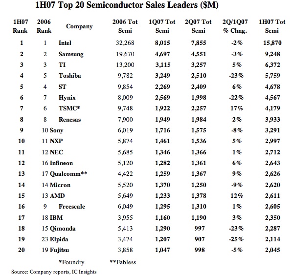
While the top three — Intel, Samsung and TI, retain their positions, ST and Toshiba have exchanged the next two positions, as have Hynix and TSMC, while Renesas remains at no. 8!
Freescale has taken a big drop from no. 9 to no. 16, while Sony, NXP and NEC gained one place each. Infineon has climbed back up to no. 12, from no. 16, while Qualcomm occupies the no. 13 position, up from no. 17. AMD dropped two positions, from no. 13 to no. 15.
Will the semicon industry see a tight year ahead? As per reports, IC Insights said that there should be a “noticeable seasonal rebound” in overall IC demand beginning in September 2007, which may cause “significant changes” in the top 20 semiconductor ranking in the second half of 2007. Wait and watch this space!
