Archive
ISA, UK-TI MoU to develop semicon industry
 Recently, the India Semiconductor Association (ISA) signed an MoU with East of England International (EOEI) to promote and develop the semiconductor industries in their respective domains.
On August 31st, which is early next week, the ISA and the UK-TI will be signing an MoU to extend this relationship further.
My colleague, Usha Prasad and I met up with Chandrika Anil, Manager – Membership Services, ISA, to hear more about the MoU.
Elaborating on how the MoU between the ISA and UK Trade & Investment (UK-TI) is going to help in encouragement and development of Global Value Chain Partnerships, Chandrika said that the ISA and the UK-TI share a mutual interest to promote and develop the sector semiconductor industries in their respective domains. The MoU between ISA and UK-TI entails promotion of the concept of Global Value Chain Partnerships.
As part of the MoU, the two organisations have agreed that:
- Global Value Chain Partnerships are of mutual benefit in the ongoing development of the Indian and UK semiconductor industries and the relationship between them.
- ISA and UK-TI will co-operate with each other in the following activities to encourage and develop Global Value Chain. Partnerships between Indian and UK semiconductor firms. This allows for:
- Promoting the concept of Global Value Chain Partnerships amongst the Indian and UK semiconductor industries in the most appropriate manner
- This may include website, newsletters, conferences and direct discussion with firms.
- Identifying, through ongoing research and discussion, areas of potential business opportunity which could be addressed by Indian and UK firms working together
- These areas could form a set of themes around which ISA and UK-TI may wish to focus on seminars and other activities to raise awareness, understanding and interest.
- Encouraging firms in the two industries to register (free of charge) their interest in exploring relevant partnerships and business opportunities in the identified areas
- This would involve inviting firms to provide information about their interests and capabilities, periodically reviewing identified opportunities which may be relevant
- Facilitating meetings between firms and groups of firms to take forward discussions with a view to formation of Global Value Chain Partnerships
The MOU will create a synergy between India and the UK in the areas of design, device and applications.
You can read more on ISA’s website. Thanks for the interaction, Chandrika, and well done, Usha!
Global semi to dip by 28pc in 2009; Indian semi to grow at 13.4pc by 2010! Don't get carried away!!
Contrasting numbers, isn’t it!
Let’s start! Yesterday, Malcolm Penn, CEO and founder of Future Horizons, said at the International Forecast Seminar (IFS) in London that the global semiconductor market will fall by 28 percent in value and by 26 percent in unit shipments in 2009 after the unprecedented collapse of Q4 2008.
Penn has added that Q2 2009 will be the bottom of the dip, with a 15 percent increase forecast for 2010 and 28 percent in 2011.
This afternoon, the India Semiconductor Association (ISA) released the ISA-Frost & Sullivan report update 2008-10″, the third report on the subject and the second update, which stated that the total revenues of the Indian semiconductor market are likely to grow from $5.9 billion in 2008 to $7.59 billion in 2010 at a CAGR of 13.4 percent. The total available market (TAM) revenues are anticipated to climb from $2.53 billion in 2008 to $3.24 billion in 2010 with a CAGR of 13.1 percent.
Be aware that these numbers do not include India’s strength in embedded and design services. This will be covered in a separate report. Nor do these numbers include any potential growth for India in the solar photovoltaics space, which also has its separate report.
Now, these ISA numbers should make anybody wonder: the Indian semiconductor industry is in for a boom time! Far from it!! India’s contribution to the global semiconductor industry is still quite small for it to really make an impact.
Some other points to note!
First, according to the ISA-F&S update, the decline in CAGR, from 26.7 percent, in the earlier report of 2007, to 13.4 percent, in the current report, is on account of revised investment and manufacturing scenario seen in the second half of 2008.
Also, as Ms Poornima Shenoy, president, ISA, indicated: “India is a story of growth and this is important in such times though growth may be below past projections. The current slowdown will impact manufacturing investment prospects. A low manufacturing index for electronic products leads to higher imports and thus lowers the local potential for semiconductors, their key component.”
Next, India’s electronics industry manufacturing index of just 0.39 forecast for 2010 will result in an opportunity loss of $4.35 billion for semiconductor sales in India.
I haven’t seen many new start-ups and Indian product companies. While IT/office automation (IT/OA), wireless handsets and communications segments are going to define the semiconductor market growth, it remains to be seen how much of these come out from Indian, home grown companies. Perhaps, Indian entrepreneurs are averse to risk taking in semiconductors. We also have India’s wafer IC fab story, which didn’t really take off as expected.
It would be advised not to overlook these points and rejoice in the numbers for the Indian semiconductor industry. We still have many, many miles to go!
I would personally be much more pleased, and am sure, most of you will agree, if all of these numbers for the Indian semiconductor industry came more from the Indian based companies, rather than the Indian arms of multinationals. Besides, I am still waiting to see what sort of steps are being taken to incubate such companies.
I will be writing more about the global and Indian scenarios in depth, especially, the Indian scenario, in separate posts.
Why solar/PV is good for India? An ISA perspective!
 Recently, the India Semiconductor Association (ISA) held an educative briefing session on the potential of the solar PV market in India, which was conducted by Rajiv Jain, Director, Government Relations, ISA.
This meeting was held well before iSuppli issued a warning that there could be global solar sunburn in 2009! I am sincerely hoping that most of the points mentioned by ISA’s Jain still hold good in the coming year, and that India really does well and takes off in solar photovoltaics.
The ISA’s vision: To help make India an attractive global destination for PV manufacturing and a world leader in solar energy.
Starting with the basics of photovoltaics, he said that it is a package of solar cells used to convert energy from sun to electricity. In simpler words, photons from sunlight knock electrons into higher state of energy, thus creating electricity. The electricity can be used to power equipment or recharge a battery. A typical PV system mainly consists of a PV module, battery, inverter, controller and junction box.
Focusing on the technological landscape, he touched upon the two key technologies for solar: crystalline and thin film.
Crystalline silicon is said to be the most mature Si wafer technology, with the largest market share. Though, high on cost, it has a typical efficieny of 14-18 percent. Crystalline silicon is said to suitable for rooftop applications.
Thin film is nothing but thin layers of photosensitive materials on glass. It is currently on high growth due to silicon shortage, and very low on cost due to low material consumption. The efficiency is about 6.5-8 percent.
A third technology, nanotechnology, is the future technology for cost reduction. It is more in the R&D space as of now.
Present scenario for solar
So what’s the present scenario? In 2007, of $71 billion invested in new renewable energy (RE) capacity globally, 30 percent was in solar PV. It is the fastest growing area in the energy sector, with a CAGR of 47 percent over the last five years.
Grid-connected solar PV has been high growth market segment in 2007 (50 percent increase). Also, 86 percent of the PV installations are largely in four countries, with Germany at 47 percent being the outright leader.
Market drivers are said to be attractive feed-in tariffs, national PV market development and acceptance, RE obligations through solar PV, access to cheaper mode of finance, manufacturing incentives as well as strong R&D.
Why solar for India
I have addressed this in an earlier blog post. Here’s what Jain had to say, and it is mostly in line with the earlier discussions.
First, India has among the highest solar irradiance globally. It also has the best quality reserves of silica in Orissa and Andhra Pradesh. India has also established itself low cost producer and assembler of solar PV cells and modules.
The major challenges include attaining scale and integration for cost reduction, and, R&D for development of the industry.
Solar insolation in India
To start with, the daily average solar energy incident varies from 4-7kWh per m2. Next, we have multiple sites with solar irradiation >2000 hours per year. In contrast, Germany has 900-1,200 hours per year. Further, most parts of India have 300-300 sunny days in a year translating into a potential of 600GW. Also, potential in some states like Rajasthan is 35-40 MW per m2.
It is well known that the Indian semiconductor policy of 2007 has triggered off the now well publicized efforts in solar initiatives. The government of India has received 16 applications with investments envisaged at app Rs. 1,55,000 crores.
The investments in solar PV manufacturing exceed Rs 1,25,000 crores. Generation based incentives (GBI) are going to be key.
Potential market segments in India
There are quite a few, actually. In rural electrification, the government of India’s target is to achieve ‘Electricity for all by 2012’. About 18,000 remote villages will likely be electrified through RE. About ~25 percent of the remote villages, i.e., 4,500 villages, form a very viable market.
Next comes telecom back-up power! PV is a cost effective alternative to diesel generators (DG) for back up power for shorter duration, as DG based systems suffer from several disadvantages.
Another key market could be grid connected solar PV based generation. Current tariffs do not provide attractive IRR to developers. Decreasing system prices are however, likely to improve the economics.
Finally, roof based BIPV is said to be an alternative to reduce the cost of power procured by commercial buildings.
ISA’s recommendations
The ISA has also made salient recommendations via its report on the industry. These include areas such as manufacturing: with an aim to encourage companies investing in ‘Scale and integration’, provision of capital subsidy to larger number of units, availability of funds at a cheaper rate, and an emphasis on R&D.
Also, the ISA has recommended that GBI be given for a tenure of 20 years, with the present period being 10 years. Further, it has suggested an accelerated depreciation along with the GBI scheme, and the availability of GBI for an unlimited capacity for a period of five years. The ISA has recommended an enactment of the RE Law requiring utilities to progressively increase power purchase from RE.
On its part, the ISA has been working with the government of India and various state governments as well. It has a sound rapport with concerned ministries – MNRE, DIT and NMCC.
The ISA has also assisted in the technical evaluation of solar PV proposals received in Fab City, Hyderabad. It has also drafted a semiconductor policy for the government of Karnataka, which should be out early next year, hopefully. The ISA is also working with several other state governments to promote the industry in their states.
The second ISA Solar PV Conclave is scheduled for November 2009 at Hyderabad.
Very good intentions, all of these! Now, for the Indian industry and the government to deliver, and walk hand in hand!!
Solar/PV is just right for India
There have been significant investments in the solar/photovoltaic space in India in the recent past, and that does not look like ending any time soon.
Given the ongoing global financial crisis, and the state of the global semiconductor industry, it appears that India has bet quite successfully on the solar/PV segment. In fact, it seems that solar/PV is just right for India! In fact, it may just kick off the kind manufacturing activity India really needs.
Poornima Shenoy, president, India Semiconductor Association (ISA), says that solar/PV is right for India for a variety of reasons.
Firstly, India has among the highest solar irradiance, globally. Secondly, it is established as a low-cost producer and assembler of solar PV cells and modules. And thirdly, India has among the best quality reserves of silica in the states of Orissa and Andhra Pradesh.
She adds: “At present, solar PV may not seem to be an attractive option, primarily due to high generation costs. However, in the coming years, with increases in fossil fuel prices, rising environmental concerns, and a reduction in the cost of solar PV technology, it is likely to become a major source of energy.”
The ISA expects 2015 to be an important year for the solar/PV industry. Around this time, the product cost of the Indian solar PV industry is likely to match the semi grid parity (peak power) globally, and also to match the grid parity within India.
The four major segments offering maximum potential in the coming years for solar PV in India are: rural electrification — decentralized distributed generation (DDG); grid interactive solar PV power plants; backup power for telecom (base transceiver stations); and roof-based solar PV systems.
ISA-NMCC report on solar/PV
The ISA recently released a report on the solar PV market in New Delhi with NMCC (National Manufacturing Competitiveness Council).
According to the ISA-NMCC study, of the US$71 billion invested in new, renewable energy capacity globally in 2007, 30 percent of was in solar PV. Solar PV is the fastest growing area in the energy sector, with a CAGR of 47 percent over the last five years. The grid-connected solar PV segment saw 50 percent growth in 2007.
As per the report, the solar PV industry is likely to grow four-fold by 2011. However, there are various uncertainties in the short- to medium-term on both the supply and the demand side.
On the supply side, the main constraint is the lack of available polysilicon. The demand side is limited by the quantum of incentives for solar PV.
Gradually, there will likely be improvements in technology. The decreasing cost of manufacturing could drive the preferential tariffs lower, and ongoing demand for PV products could also attract significant investment.
As for the global solar PV supply chain. Thin-film production is one of the fastest growing segments in solar. The lack of available polysilicon is limiting growth, and this has led to the emergence of thin-film technology. This technology has enjoyed substantial growth since 2005: 80 percent in 2006 and over 100 percent in 2007.
Bangalore not cowed down by serial blasts, ISA Excite a success
Friends, I am really pained to report that Bangalore has been rocked by eight-nine serial blasts of low intensity today! As per the TV channels, there have been two deaths and several people injured. This is extremely unfortunate!
Countrymen and women, please join me in condemning this dastardly act of the serial blasts in Bangalore today.
I would also like to add a message sent to me by a good friend, Xavier, which says: Bangalore, don’t be cowed down!
This is a small gesture that goes out to send the right signal to those who are keen to take away our freedom, our right to live peacefully for whatever their ideology is!
“Let our thoughts and prayers be with the near and dear ones of those killed and injured in these blasts.”
Those who indulge in such activities are cowards. While such acts are meant to create panic, Bangalore has stood firm! Yes, people across the city, in various offices and other establishments, left home early, more so as a precautionary measure, telephone lines were jammed for some time, and there were the usual traffic jams — largely due to the rains. However, there has been little panic. Yes, there may have been panic in the affected areas for some hours post the blasts.
In fact, I wasn’t even aware of the blasts as I was attending a wonderful event on semiconductors — the ISA Excite — with a colleague, Ravinder, at Leela Palace. We only learned of the blasts on reaching office! Interestingly, there were little signs of panic on the roads as we were driving back to the office! Well, I’ve had quite a few phone calls and messages, thereafter! Am sure, it’s been the same for nearly everyone in the city.
The country has gone on high alert since the blasts, as these can actually happen anywhere! However, India is a strong country, made up of very strong-minded people. Such acts of cowardice will not stop the normal pace of life. At best, normal life could be disrupted for a few hours.
Of course, a lot needs to be done to secure the IT capital of India, and possibly the world. It is hoped that the security agencies in India would do everything within their capability to ensure that such acts are not repeated. The damage could have been far greater, and some even wonder, whether there is some sort of a hidden message behind today’s serial blasts.
Going back to the ISA Excite event, organized by the India Semiconductor Association, it was really heartening to learn that the Karnataka state will soon have its own semiconductor policy. I will be blogging more on this later tonight or tomorrow.
I’d also like to mention that the ISA Excite event was a very strong indication that the Indian semiconductor industry is very healthy and doing well, although, we may not yet have a wafer IC fab, and there are infrastructure challenges to mount.
Nearly everyone from the Indian semiconductor fraternity was present at the show. I am sure, several people heard about the blasts, and expressed their disgust at the happenings. However, the show went on! When the going gets tough, the tough get going. It was a message from the Indian semiconductor industry that even in tough times, it will move forward.
The show must always go on! And successfully!
India leads world in semicon: S. Janakiraman
 Irrespective of the debate raging within the semicon community regarding the IC wafer fabs in India, the strength of and the talent within the Indian semiconductor industry has never ever been in doubt.
Delivering the welcome note at the recently held ISA Technovation 2008 awards ceremony at the Indian Institute of Science, S. Janakiraman, the former Chairman – India Semiconductor Association, and President & CEO – R&D services, MindTree Ltd, elaborated the fact that India now leads the world through execution of most complex and latest technology designs.
Former president of India, Dr. APJ Abdul Kalam was the Chief Guest at the function.
Commenting on the ISA’s role, Janakiraman said that it has been an industry driven body focused on the unique needs and progress of the semiconductor and related industries in India to make it vibrant and project India as a global leader. The ISA’s journey began four years back, in late October 2004, in Bangalore, under the mentorship of Dr. Sridhar Mitta, when like minded industry leaders gathered together and debated how India can achieve leadership position in the semiconductor space similar to IT and software.
Janakiraman said: “We have come a long way since then and today ISA is recognized by everyone in the country and all such bodies outside, as the sole representation of the Indian semiconductor industry. This has been a significant achievement and made possible by all.”
Today, there is a good presence of both Indian and MNC organizations, large as well as start-up companies, design, as well as manufacturing organizations, with the members of ISA now totaling 130! The ISA also works closely with central and state governments to give shape to the aspiration of our industry. It had played a key role in framing the semiconductor policy that enables larger investments in the semiconductor manufacturing ecosystem.
He added: “India has excelled in areas that are knowledge intensive. Semiconductor design is no exception, and today, we lead the world through execution of most complex and latest technology designs. The market size of the IC design and embedded software industry in India was $6 billion in 2007 and has the potential to grow into $43 billion by 2015. It currently employs around 130,000 engineering professionals.”
ISA Technovation Awards
One of the primary charters of the ISA is the talent initiative. This initiative focuses not only on generation of quality talent aligned to the needs of the industry, but also to recognize innovation and research, that further nurtures talent.
The Technovation Awards were created in 2007 to recognize excellence in Academia that has made us what we are today. These awards have been created to honour semiconductor research in India and to create role models in core technology areas.
The award categories are:
1. TechnoVisionary for life time achievement in the semiconductor area
2. TechnoShield for research entity, lab or a department for excellence in a semiconductor domain of interest
3. TechnoMentor for recognizing academician/researcher for contribution in the semiconductor area
4. TechnoInventor for individual excellence in doctoral/masters researchers
This year, ISA has created two special awards for recognizing researchers from Karnataka which have been instituted by VLSI 2007 committee, under two categories:
1. Best Faculty award
2. Best PG student award
The number of nominations went up multifold in this year and an able set of panelists had a tough task of selecting the award winners.
“Given the vibrant scenario of the industry and importance of the event, we have our great leader and visionary Dr. Abdul Kalam with us today evening to recognize the award winners in person'” added Janakiraman.
“Dr. Kalam had been a role model especially for the younger generation – who are the future of this country. Dr. Kalam has been a visionary and a great inspiration for the community present here. It is a great honour for ISA to have Dr. Kalam amongst us.”
The Award Winners @ Technovation 2008
Technovisionary
Juzer M. Vasi, Deputy Director, Indian Institute of Technology, IIT Bombay
TechnoMentor
Bhargab B. Bhattacharya, Professor and Officiating Deputy Director, ISI Calcutta
TechnoShield 2008 (Rolling Shield)
Indian Institute of Technology, Madras — Semiconductor Devices Circuits & Systems Group (SDCS)
TechnoInventors
(Ph. D category)
Debdeep Mukhopadhyay, Indian Institute of Technology, Kharagpur
Thesis : Design and Analysis of Cellular Automata Based Cryptographic Algorithms
BP Harish, Indian Institute of Science, Bangalore
Thesis: Process Variability –aware Performance Modeling in 65 nm CMOS
D. Mahaveer Sathaiya, Indian Institute of Technology, Madras
Thesis: Modeling of Gate Leakage in Aigan/Gan hemts and nitride oxides
(M Tech category)
Rakesh Gnana David J, Indian Institute of Science, Bangalore
Thesis: Adaptive Keeper Design for Dynamic Logic Circuits Using Rate Sensing Technique
Nayan Bhogilal Patel, Indian Institute of Science, Bangalore
Thesis: Performance Enhancement of the Tunnel Field Effect Transistor for Future Low Stand-by Power Applications
Former president of India, Dr. APJ Abdul Kalam, Chief Guest at the function, advised the Indian semiconductor industry to develop tailor-made chips so that electronic equipment could become more cheaper and competitive.
India fab story not disappearing: SemIndia
 According to B.V. Naidu, managing director, SemIndia Systems, and Vice Chairman – India Semiconductor Association (ISA), the Indian fab story is well on track. Here, he speaks about the FabCity, the status of fabs in India and SemIndia’s initiatives.
On the status of setting up of IC wafer fabs in India, he says that a couple of companies are in the process of raising the money for setting up the wafer fab in India. We still do not know the timelines for the same.
On India’s fab story is disappearing, Naidu feels that it is always difficult to raise the money for such large capital-intensive projects, which are happening first time in the country. “One of the large industrial groups also announced their plans to set-up the fab. This shows that the fab story is not disappearing,” he says.
The Andhra state government had recently sent notices to SemIndia and NanoTech over FabCity. Pertaining to the status of the project, he adds that any capital-intensive new projects of this kind will take some time. It is also quite natural that the government generally issues such notices more to put pressure so as to expedite the project implementation. It is good that the governments are closely monitoring the progress of the project implementation.
According to him, SemIndia’s ATMP project construction has started. The FabCity has already come-up and many solar PV fabs are being set-up in the FabCity. This shows that efforts of SemIndia, ISA and the government of AP have yielded the successful results to make FabCity a successful project.
The India Semiconductor Association (ISA) can only indicate that such government communications are common for wherever there is government support. The ISA will continuously put in their efforts for attracting the new investments to India and work along with the governments to make sure that their efforts are fruitful.
“SemIndia’s ATMP project construction has started and we are still looking for the investors for their fab project,” says Naidu.
So, what sort of planning is now required from the Indian semicon industry? As per the SemIndia managing director, the Indian semicon industry should continuously work with the government to make sure that the government of India’s semicon policy is successful and efforts are various state governments in attracting the new investments in this area are fruitful.
The ISA will continuously strive for creating the balanced eco-system for the semicon design industry, high-tech manufacturing and talent nurturing.
India's growing might in global semicon
It is no longer a secret that India is fast becoming the world’s destination, and increasingly the source too, for semiconductors. India also shows the most rapid growth potential among the BRIC countries.
Speaking at the recently held International Electronics Forum (IEF) 2008 at Dubai, organized by Future Horizons, S.Janakiraman, the outgoing Chairman – India Semiconductor Association, and President & CEO – R&D services, MindTree Ltd, touched upon India’s growing might as a being the third largest country in terms of purchasing power parity, as well as its growing presence in the global semiconductor industry.
It is no surprise that the current market drivers in India happen to be mobile phone services, IT services/BPO, automobiles and IT hardware. Add to these are the facts that India is very strong in design tools, system architecture and VLSI design, has quite strong IP protection laws, and is quite strong in concept/innovation as far as the semiconductor industry is concerned.
Testing and packaging are in the nascent stage. While India lacks a semicon wafer fab, as of now, there have been several announcements regarding solar fabs by leading firms such as Videocon, Moser Baer, Reliance, etc.
In the electronics manufacturing domain, India’s strength lies in hardware, embedded software and industrial design, OEMs, component distribution (includes semiconductor and box build), and end user/distribution channel, as well as more than moderate strength in product design and manufacturing (ODM, EMS).
India is likely to witness $363 billion of equipment consumption and $155 billion of domestic production by 2015. India’s electronic equipment consumption in 2005 was 1.8 percent. It is likely to grow to 5.5 percent in 2010 and 11 percent in 2015, as per a joint study conducted by the ISA and Frost & Sullivan.
The Indian semiconductor TAM (total available market) revenue is likely to grow by 2.5 times while the TM (total market) is likely to double revenues in 2009. The TAM is likely to grow at a CAGR of 35.8 percent and the TM is likely to grow at a CAGR of 26.7 percent, respectively, during the period 2006-09.
Telecom, and IT and office automation are currently the leading segments in both TM and TAM. Consumer segment occupies the third fastest growing area in the TM, while the industrial segment is the third fastest growing area in the TAM.
The major semiconductor categories include microprocessors, analog, memory, discrete and ASIC, while the major end use products include mobile handsets, BTS, desktops, notebooks, set-top boxes and CRT TVs.
Emerging base of EMS firms
India is also becoming an emerging base of EMS companies, thereby completing the electronics ecosystem. Five of the top 15 EMS companies globally have set up their manufacturing facilities in India. These include Celestica, Elcoteq, Flextronics, Jabil Circuit and Solectron. Two other large companies are in the process of setting up plants — Hon Hai Precision Industry and Sanmina-SCI.
Nokia has set up its manufacturing facility as well. It has invested $210 million in the plant since January 2006. The India plant has set another benchmark of achieving the fastest ramp up across all Nokia facilities worldwide. Currently, approximately 50 percent of the production from the plant is consumed domestically and the rest is exported to other countries.
Indian embedded design industry
The Indian embedded design industry has been going from strength to strength. The recent IDC-ISA report puts revenues from India’s VLSI, board design and embedded software industry to grow to $10.96bn by 2010 from the current $6.08bn in 2007.
As of 2007, embedded has 81.1 percent share, hardware board design 6.3 percent; and VLSI design 12.3 percent, respectively.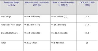 Source: ISA.
The challenges and focus areas for the embedded design industry include manpower — focusing on increasing productivity, creating readily deployable engineering workforce, and focusing on developing high-end skills.
Another area India is working on is moving up the semiconductor value chain. India is now focusing on end-to-end product development, investing in IP development, developing India specific products, and partnering with OEMs to understand the market needs.
The challenge is posed by the cost structure. India needs to better address cost management, i.e., increasing infrastructure and salary costs, as well as managing the dollar’s impact.
India design inside
Several global products have been now developed out of India. Some recent examples are: Harita Infoserve Ltd is developing interior parts and conducting computer tests on components for General Motors Corp.
Next, Ittiam’s videophone design will become almost entirely an India story: part of the chip, the product design, the software and, finally, the manufacturing also done here. Plexion Technologies has worked on the interior design and windows for a DaimlerChrysler (DCX) bus.
Quasar Innovations designed and developed a dual SIM card — PTL910 mobile phone for Primus, to be launched in the European market. The mobile phone allows the user to have SIM cards from Primus for two countries, with the phone automatically choosing the correct SIM depending on the user’s location.
Finally, MindTree itself has designed a feature rich satellite handset with mobile handset form factor for a European company.
Attractive semicon policy
India’s semiconductor policy is likely to attract investments of over $10bn. The government of India will bear 20 percent of the capital expenditure during the first 10 years for units located inside SEZs and 25 percent for those outside.
For semiconductor manufacturing (wafer fabs) plants, the policy proposes a minimum investment of $625mn. The same for ancillary plants would be $250mn.
The government’s participation in the projects would be limited to 26 percent of the equity portion. The key benefit here is the grant of the SEZ status.
India’s evolving ecosystem is driven by the bottom of the pyramid (BOP) opportunity. Tata Motors announced the now famous Nano — the Rs. 1 lakh (sub $2500) car -– said to be the world’s cheapest car. This has been indigenously developed in India, for India, by Tata Motors.
Nano has passed all mandatory crash tests and Euro IV norms. It is likely to be commercially launched in the second half of 2008.
All of these make India the most happening semiconductor and electronics destination. Don’t be surprised if companies not having an India strategy in place miss out on the action!
