Archive
What India now offers to global semicon industry!
This semicon blog post is very timely as I keep getting a lot of questions on the topic: what does India NOW offer to the global semiconductor industry in this recession! In fact, several industry friends asked me this question during the recently held ISA Vision Summit 2009.
By the way, I have two good sessions from the ISA Vision Summit 2009 to blog about, and those will happen after this post! So, stay tuned folks!! 🙂
Back to the key question: What does the Indian semiconductor industry now offer to the world?
 My quest for answers took me to S. Janakiraman, former chairman, India Semiconductor Association (ISA) and President and CEO-R&D Services, MindTree. Incidentally, Jani Sir, had highlighted some time ago that despite the lack of wafer IC fabs, fabless India continues to shine brightly! And, I agree with him! Even at Dubai last year, during the IEF 2008, Jani Sir had talked about India’s growing might in global semicon. I consider him to be the right person to discuss how India should frame its semicon path forward.
According to Jani Sir, we will remain in a tough economic scenario for some more time to come. “The cost of R&D, be it development or re-engineering or support is critical for the survival of semiconductor companies, but all of this needs to be done at lower costs. India will continue to be a cost leader to get more engineering done at the same cost or the same engineering done at a lower cost. India will continue to be a safe haven for such investments,” he contends.
India itself is a high growth market that will get sizable in the next five years for the semiconductor companies. No one can understand India and the emerging market requirements than the companies who are located here. That can be leveraged by the world to create value for many products that will serve the emerging market needs.
Janakiraman said: “Indian companies are also investing in technologies and creating intellectual properties/building blocks of technologies. These are the essential elements to create products/solutions in a shorter time-frame when the market starts recovering and builds up the appetite for consumption. Hence, Indian companies need to invest more in such areas and position themselves as value-add vendors to source technologies.”
Newer markets such as electronics in healthcare and renewable energy space provides a level-playing field since India’s maturity level is no less inferior to the western world. “We need to invest, and create solutions and products that can establish India not only as a market, but also a leading technology provider for the global market,” Janakiraman advises.
Has Indian semicon lost its way a bit?
Some folks believe that the Indian semiconductor industry has slightly lost its way since the SemIndia fab debacle late last year. I’ve mentioned earlier that hardly anyone wants to speak about having fabs in India at this point of time. Nevertheless, we’ll need to explore whether the Indian semiconductor industry is still on track!
According to Janakiraman, while the global consumption of semiconductors has seen a drastic drop in Q4 of 2008 and is likely to see a negative growth in H1 of 2009, India will be one among the few markets that will see an increasing consumption through the sales of electronic products.
He added: “The captive and design services companies serving the semiconductor market are facing a head wind, no doubt. However, the impact on them is much lesser compared to what is happening in the rest of the world.”
With the Indian semiconductor market continuing to grow, while the global market is in decline, it is possible that India may end up seeing a slower growth, but with an increased market share.
Janakiraman said: “I see the dynamics in the market will lead to India gaining way for the longer term, even though we can’t escape the short term pains. When the recovery starts, India will gather much stronger and faster momentum of growth as it will be a lucrative market for selling and the lower cost market for sourcing for any of the global semiconductor players.”
Finally, what really needs to be done to get the industry in India buzzing? For starters, don’t give up hope!
Added Janakiraman: “Look at it as an opportunity to get into a level-playing field rather than a losing ground. Consider India as a potential future market. Look at and invest in the emerging opportunities such as healthcare/security/energy, and build products like telemedicine, surveillance systems and power management systems. Invest in idea creation and product management systems, and get ready for the new model of business when recovery starts.”
I wonder why Jani Sir didn’t deliver the keynote at the ISA Vision Summit 2009! He is just the right person as far as propping up Indian semicon is concerned!!
Can the Indian semicon industry dream big? (And even buy Qimonda?)
I had ended one of my previous blog posts by saying whether the Indian semiconductor industry was hitting the right notes?
In a continuation to that specific thought, it is necessary to first examine where India stands in the global industry. We are very strong in embedded design and design services — our traditional strengths. While these will hold good for a long time, these are probably not enough to really help India make a serious mark at the global level.
The Indian semiconductor industry, in its current state, needs a rethinking as far as strategy is concerned. Maybe, it cannot survive on chip design alone. Especially in times of downturn, the global semiconductor industry players would be looking for new markets and even customers, rather than low-cost production centers.
Consider these points: In the current economic environment, is the interest in developing new business relations with India really a top priority for overseas companies? Probably not, at this very point of time!
India is also seen more as a source of resource; and the extra resource is the last thing firms need at the moment, given the recessionary climate. What global firms are looking for are new markets and customers, and these points, along with its infrastructure, have been the areas of Indian weaknesses. Maybe, all of this will change, but definitely not overnight! And it needs some more planning.
That leads me to an interesting comment from a reader of my article on CIOL, who went on to suggest that an Indian investor could consider buying Qimonda!
Now that is some serious thought and vision as far as mid- or long-term planning is concerned. However, will there really be any takers for this? If this really happens, fabs can be built in India for memory production. If these fabs perform well, it just might turn out to be a good investment in the mid-term future of the Indian semiconductor industry. Definitely, it will make the world sit up and take notice. The other players would surely give India a look-in thereafter.
Quite a thought! This suggestion of investing in Qimonda is indeed a vision. Can the Indian semiconductor industry develop the courage to show and work toward making this kind of a vision a reality?
What should India do to develop products? Speaking with Anil Gupta, managing director, India Operations, ARM, is always a pleasure.
I asked him: Does India have the capability to sustain or even build a product development ecosystem? What needs to be done?
He said: “We need the following for this:
* Entrepreneurs committed to product development and willing to take that risk;
* Investors willing to take risk on product development companies;
* Consumption, and this will happen as the economy improves any way, and
* Deep enough technical/technological knowledge/know-how to put reasonably competent end products together.”
According to him, all of these qualities exist in India, and he cited examples of companies such as Sukam, Tejas, etc.
Well, there you have it!
We need enterprising entrepreneurs in India who are committed toward product development and willing to take that risk, especially in semiconductors. We need investors who can believe in things like even buying Qimonda, or some other company. After all, isn’t this what everyone’s been saying: this is the time to buy!
Dream big, India!
TI Beagle Board for Indian open source developers and hobbyists
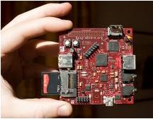 Texas Instruments recently introduced the pocket-size, USB-powered Beagle Board based on TI’s OMAP3530 applications processor. It features an ARM Cortex-A8 core, 2D/3D graphics engine and high-performance TMS320C64x+ digital signal processor (DSP) core.
This will help open source developers and hobbyists in India to realize their creative design ideas without being restricted by expensive hardware development tools, lackluster performance capabilities, high power consumption or stifled design environments, according to Khasim Syed Mohammed, Lead Developer for Open Platforms, Texas Instruments India Pvt. Ltd.
He added: “It helps us in learning cutting edge technology, innovating new ideas and executing them. Beagle board should be used to explore the growing demand in areas like medical, security, infotainment, navigation, education, signal processing, mobile devices and communication.”
Important for India
This initiative is particularly important in India where students can use the board to learn, show case their efforts and global recognition for their innovations.
Innovators in India should use this opportunity to prototype their ideas using the specification software hardware openly available in a never before package. It is important for the student community to learn new technologies, explore new areas and innovate. This initiative by TI also helps startups in India who want to explore the OMAP hardware but have limited support base for their requirements.
Passionate open source developers and hobbyists in India can realize their creative design ideas without being restricted by expensive hardware development tools, lackluster performance capabilities, high power consumption or stifled design environments.
Open platform innovators have the expandability of desktop machines without the expense, bulk or noise with the Beagle board, which is a powerful, low-cost and fan-less embedded system development board smaller than the size of an index card.
Board named after Beagle
The board is named after a popular breed of dogs, Beagle. It has been designed it to be one of the shortest pocket sized OMAP3530 boards. TI is encouraging the Open community to treat this as a pet, which is easy to carry and can be USB powered so that development is made easy and can perform high end applications at very less power.
Inspired to create a small, open source development board, a small group of enthusiastic engineers worked together on the concept and realization of the Beagle board. The resulting 3×3-inch board bridges desktop and embedded development by allowing developers to use the same peripherals and usage mode for almost limitless expansion. Developers are able to design exactly according to their specifications and collaborate with the community on creative new applications.
Mohammed said: “There is a growing need for development support in the Open Community. The Open Community is capable and passionate to work on industry’s high end processors and architectures and build innovative applications and prototypes for mobile, portable infotainment, portable navigation, medical, home security and many such applications. Another important reason for this initiative was the cost implications in owning a high end platform which was restricting them in exploring many such ideas/applications.”
Beagleboard is a global initiative to address the growing needs of the Open community to help them innovate and explore new areas by providing them access to leading hardware and software, giving them a forum to present their views and thoughts, showcasing their efforts for global appreciation, maintain community’s contribution.
Developers can quickly maximize their design concepts by tapping into the expertise and support of some of the industry’s top Linux programmers already experimenting with the Beagle board. With communities hosting the latest updates and codes, live forums and chats for easy collaboration, developers have easy access to support and exchange of ideas. Users are encouraged to join active, existing communities already participating in the project.
iPhone's impact minimal on chip market
Future Horizons recently released its Global Semiconductor Monthly Report June 2008.
The first question on everyone’s minds is: Are there finally any signs of the global semiconductor/chip industry turning around. Malcolm Penn, CEO, Future Horizons says that most of the evidence is still anecdotal. The real, clear proof will show itself in Q3-08.
There are a set of market fundamentals that are in remarkably strong form. The global economy still strong, and even showing signs of ‘not getting worse’ in the US. However, there is also tight fab capacity. No matter, the unit demand has been holding firm and ASPs are holding no longer in free fall.
Even the memory market has been holding up much better for now. Penn says that memory ASPs have been ‘flat’ for six months now. So, there has been some upward movement in ASPs. According to Penn, memories have been flat, and are no longer falling. The logic has been increasing, but micro is still falling, and the overall total ICs is trending up.
The impact of Apple’s iPhone 3G has been minimal so far on the chip market. Penn says: “It’s just one item in a very large and complex mix of products. The overall i-phone volume is miniscule,” adds Penn.
With several advancements and announcements happening in the solar/PV segment, it may seem that the solar/PV market is taking over from where the chip market slipped. Penn says that although it certainly is a growth market for the equipment suppliers, but with still very small numbers, it cannot make up for the semicon equipment/capex slowdown.
Future Horizons had earlier forecasted 12 percent growth for the global semiconductor in 2008. With some other analysts revising forecasts, let us examine whether Future Horizons consider a revision as well.
Penn says: “If I were doing the forecast now, I’d have probably settled on 10 percent rather than 12 percent, but this is fine-tuning the maths, and not the analysis. We will not be changing our forecast at the July seminar.
“Our overall message is clear. The growth this year will NOT be 4-5 percent. I really do not care, if 10 percent rather than 12 percent is the final real number. We are not in the business of ‘guessing the right number’, rather, just getting the trends and analysis right.”
Penny yet to drop
Finally, there is a need to take into account the falling cap ex, tight capacity, focus on profits, continuing strong market demand, second half seasonal effects, etc. The forecast tea leaves all seem to be pointing in the same positive direction. Has the worm finally turned for the industry? Future Horizons thinks so! It also believes that the penny has yet to drop and that the impact on the market will be dramatic.
Penn explains that low capex means less new capacity (12 months later). And less new capacity means tighter supply. Tighter supply means price increases and rationing.
In parallel, falling ASPs means less profits. Less profits means an unwillingness to invest. Low ASPs means a reluctance to supply. Eventually, either someone exits the business or they increase the price.
“Positive unit growth (it is, IC units are up 9.2 percent YTD on 2007) and a positive ASP growth (so far 2008 YTD the trend is still negative 3.9, but this will reduce in 2H at least to zero, my guess is slightly positive. It is already only half last year’s decline) means strong value growth hence our belief growth will end up in the ’10 percent’ range,” he adds.
Chip market is beginning to hum again!
Future Horizons has released the May WSTS results today on the global semiconductor industry, which indicate that the chip market is slowly starting to buzz again.
 Malcolm Penn, chairman and CEO, Future Horizons, points out that as shown in May’s WSTS results, March’s sale figures romped home with a vengeance – reversing February’s lacklustre performance – with IC sales up 10.8 percent on February and 8.2 percent on the same time last year.
More importantly, the ASPs were up 13.3 percent on February and 2.1 percent on March 2007.
While the increase on February 2008 is merely part of the normal month 3 versus month 2 quarterly patterns, the increase over the same period last year is much more statistically -– and structurally -– significant.
“Finally, the chip market is starting to hum. Now is NOT the time to cut back on the 2008 forecast,” he adds.
Now then, why is the chip market exactly humming? What’s actually happened? Well, nothing specific! It is merely an overall step-by-step general improvement in everything, helped along by the normal seasonal improvement in business in the second half of the year.
So many forecasters and firms have their own forecasts. What happens now if some of these forecasts are cut or revised? Will that affect the market overall market? The answer is simple — a forecast is simply just that — a forecast — not fact! Penn says, “The market will judge whether the other forecasters’ analyses of the market were right, as it wll indeed judge whether we are right too!”
Earlier, I had blogged about Future Horizons forecasting 12 percent growth in 2008 for the global semiconductor industry. Keep an eye on that one!
Further, have the ASPs stabilized, as those are indeed a dodgy lot? Penn feels, “We believe yes, although, there will still be the normal month-on-month variations and wobbles.”
I shall continue this story in my next blog… so keep reading folks! My very warm regards and thanks to all of you who do stop by to read and comment.
VLSI as a career in India
It is a great pleasure to find people, most of whom I don’t even know, either leave comments on my blog, or even leave a post asking for help. First of all, I would like to thank all of those who read my blog posts. Two, I would like to thank a reader, Paul, for his best wishes pertaining to my recovery. Thank you friend!
I would also like to address a query left by a young reader R. Shrivatsan. It is my pleasure to let you all know that he is going to do a PG course in VLSI in Bangalore. There are lot of opportunities in the VLSI space in the country, and it would do India a lot of good if more such youngsters took to this line. India needs people with experience in VLSI!
I am not a career consultant, nor am I qualified enough to give VLSI tips to people. However, I will try and list some sites who can offer that kind of guidance to people interested in VLSI as a career.
A very good place to start looking for VLSI related information is the VLSI Society of India. This is the site that covers all that is related to VLSI. There are some related sites as well, and I am sure it would help those interested in pursuing VLSI as a career. The India Semiconductor Association is also a good place to ask around for VLSI related information.
I’d like to add that the VLSI Society of India signed an MoU with the Visweswaraya Technological University (Belgaum, Karnataka) and the India Semiconductor Association in June 2005 to spread and improve the quality of VLSI education. Under the aegis of this MoU, colleges that offer M.Tech programs in VLSI Design and Embedded Systems have been identified as centers where champions from the industry will work in close cooperation with faculty champions to improve the quality of M.Tech programs.
I also came across certain sites offering some valuable information. The VLSI Chip Design site lists some of the leading ASIC and VLSI design companies in India. Then, there is this nice little blog — India VLSI — which also has some good indications as far as VLSI companies in India are concerned.
Next, there’s a nice site — VLSI Chip Design — which also offers lots of answers, as well as news, jobs and views about the semiconductor industry in India.
Further, there a host of very good verification companies in India, such as EVE, Tessolve, etc. Lot of work is going on in this space as well. I also came across EDA 101 — a new community for electronic design engineers, managers, students and consultants whose career includes use or management of Electronic Design Automation (EDA) tools in modern digital and analog design.
There is lot of information going around on opportunities in VLSI in India. My best wishes to Shrivatsan, and hope that India gets a great VLSI engineer.
Lastly, I would like to invite knowledgeable people to send me links, etc. on any good sites, education institutes in India, pertaining to VLSI. I will publish the links and information on my blog and also acknowledge those people. Many thanks!
LabVIEW 8.5 delivers power of multicore processors
National Instruments (NI) recently released the latest version of LabVIEW — LabVIEW 8.5, which delivers the power of multi-core processors to engineers and scientists.
According to Jayaram Pillai, MD, India, Russia & Arabia, NI, new processors with multicore are coming out. Processing power is now split into two separate cores. With multicore, you are doing parallel processing. LabVIEW is a very dataflow programming tool. It is not sequential — it is decided by the data itself. And inherently, it has always been parallel processing. NI has taken the advantage from LabVIEW 5 — due to dual-core processing. It used multi-threaded architecture.
Assign different tasks on different cores
With processor technology shifting to multi-core, there is a need to run efficiently on the processor. For LabVIEW, you can assign different tasks on different cores — which are independent. They don’t have to run at the same speed. Those are the challenges multi-core seeks to address.
The technology NI has, the single application that you can build in LabVIEW, it aids in taking advantage of multicore. Part of a program can be assigned to one core. Another part is, if you don’t want to club, it can run on the another core. All of this happens on one program.
So how is the new version better? As you want to accomplish more things, you have to go to higher levels of extractions (or abstractions). The graphical program is a very high level of abstraction. You can accomplish more with the graphical programming.
Another area where LabVIEW is finding itself is in the design space. Building systems today is very complex. NI builds into three stages — design-prototype-deploy.
As an example, the Railways want to detect trains that have bad wheels. They collect data from railway lines — lot of signal processing and maths were done. NI knows how to detect defective wheels. It put sensors to that signal, go to the field and do some trials. Once you know the algorithms and the BIOS required, you can go into designing. You take the prototype and make that into a product. Each stage, in the past, used different tools.
Since it is all the way — from design to deployment — it can all be done with LabVIEW. This capability — that it can start at design and prototype, etc., brings greater value to engineers. NI call this process as graphical system design.
Community LabVIEW
Commenting on NI’s activities in India, Jayaram Pillai said LabVIEW 8.5 is a major release. “Over the last 10 years we’ve been in India, we have changed its hardware platdform. One thing that remains common is LabVIEW and what it does for scientists and engineers. We’ve been able to create a community around LabVIEW. There are users and programmers of LabVIEW. There are certified developers, companies that have been built around LabVIEW. There are applications built around LabVIEW,” he added.
Looking at graphical programming, over the last 10 yrs — the biggest challenge for Pillai has been to address customers needs for engineers who can program LabVIEW. There’s enough excitement in the market about LabVIEW. There are 1,100 jobs at least for LabVIEW.
There are people writing toolkits that can work with LabVIEW, which includes IP, developers, companies, customers, products, systems built around LabView. This has been happening within India.
Pillai said that similar to any technology adoption, there’s a take-off stage. “It is called the S Curve, and we are at the bottom of the curve. The potential is huge. Our big challenge is to be able to create more engineers in the market. I feel that over 1,000 engineers are required,” he added.
From an academic standpoint — India has about 400,000+ engineers passing out each year. Only 25 percent are hireable, with reasonable training, by companies. The IITs, state governments, etc. take care of it. That means, there are business opportunities for companies to start finishing schools for training these people for the industry.
Lots of companies are getting into these finishing schools. These students will learn about the tools that they would later need to use.
Pillai stressed that it was important how the country looks at academicians. He said: “We haven’t got into this stage as much. The IT industry has done very well and created a huge appetite for engineers. The majority of engineers passing out are hired by the IT companies.”
He added: “LabVIEW is getting accepted by people in various projects. We’ve created a LabVIEW community — the whole ecosystem.”
Outlook for 2008
According to Pillai, algorithm enineering is key during the design phase. LabVIEW 8.5 has a new tool for design stage of the graphical system design.
With LabVIEW, users can increase performance through graphical programming for multi-core processors and FPGAs. Pillai said: “At the design stage, you want to give the engineer multiple computing options. The engineer is concerned about deployment, but he would like to move from Windows to real-time. This should be done seamlessly. LabVIEW FPGA has been around for a long time.”
Programming in FPGA is not simple. NI’s offer to engineers is: look at the FPGA as a platform and program it freely without even needing to know what’s the VHDL code! LabVIEW can run on Windows, and move to RTOS and FPGA, and all of it is seamless.
As an example, Lego has a product called Mindstorm — a robot. That robot has sensors. It is targeted at 10-yr olds. On one side, a 10-yr old can program LabVIEW. All details are there in LabVIEW. On another side, it can be used in the largest, physics experiments. So LabVIEW is not complex to use.
LabView has been shipping formally since last month.
Indian designers could lead in EDA product development
 There will be the multi-nationalization of the product development process, according to Walden C. Rhines, chairman & CEO, Mentor Graphics. More executives recognize that “access to qualified personnel” is the key driver. As per A.T. Kearney Global Services Location Index 2007, India is the most attractive offshoring destination. He was speaking at the Though Leadership Forum organized by the India Semiconductor Association.
Touching on the evolution of EDA, and the role of Indian designers, Rhines said that most electronic engineers did not consider themselves “risk takers”. Most electronic engineers also don’t like to change tools and fewer even consider “hot” new tools.
On the contrary, young engineers and recent university graduates eagerly adopted new technology. It is a way for them to distinguish themselves, get the productivity advantage and they were less invested in existing methodologies.
Indian designers smart
Comparing Indian designers with the rest of the world, he said that electronic designers in India, on an average, are less experienced than in the United States, Europe and Japan. However, they are on an average, as smart, or smarter, than those in United States, Europe and Japan. There has been an increasing influence of India design centers on the multinational design flows and tools.
Disruptive change creates leadership opportunities. There has been improved power and cost through improved system architecture. The C synthesis enables faster architectural exploration and shorter time to Verilog.
C synthesis matches or exceeds hand coded RTL efficiency, as per STMicroelectronics (Reed-Solomon, Galois Field Multiplier). There have also been system architectural innovations to reduce die size — Ericsson mobile platforms. There is a need to iterate to find the optimum architecture.
Now, Indian designers have been early adopters of C-based design. The reasons were, one there was a willingness to try new approaches and two, it caused multinational parent companies to accelerate their own adoption.
India is likely to be a leader in transaction level design. They have been able to extract fast, accurate power and timing models from RTL. They have managed runs 100x-1000x faster vs. RTL, retained accuracy at the gate level and RTL, their models run with application software for hardware/software cosimulation, and they have done transaction-based verification using emulation. It has been the same for UPF-compatible verification.
Some other areas of verification where India may lead the way are assertions, coverage based verification, and algorithmic test bench synthesis.
Adoption of place and route technology
Let us see how the adoption of new place and route technology has influenced the industry. When a design flow breaks, what breaks the most often? Place and route breaks every two technology generations. Technology generations ramp to peak volume. Place and route utilizes a semiconductor company’s internal software until gate array routers emerge.
Cell-based layout requires hierarchical router with timing. Tangent attacks leading-edge 0.75 micron designs. Later, Cadence became the dominant place and route supplier at 0.35 micron as the fabless industry grew demand. [Cadence acquired Tangent in 1989]. However, at 0.25 microns, SoC drives new technology requirements. This led to the collapse of the FAM business model.
SoC needs “break” the flow. ArcSys emerged at 0.35/0.25 micron. It addresses SoC requirements for large sizes and interconnect delay. It goes public as Avant!, and is later acquired by Synopsys. However, a timing closure crisis emerges at 0.13 micron. Cadence and Avant!/Synopsys try to extend older tool architectures.
Now, timing closure “breaks” the design flow. At this point, Magma emerges at 0.13 micron with timing-driven layout solution. At 90nm, Magma dominates timing-driven design. It also approaches Cadence, Avant!/Synopsys place and route market share. What the industry witnesses is that a new problem emerges and a new, leading-edge solution provider enters every two nodes.
And now, pressures are creating 65/45nm discontinuity. These are process and design variations, low-power requirements, and large design data sizes. Explosive growth in complexity requires multi-corner, multi-mode analysis.
Achieving power/performance design goals requires analysis of corner cases for manufacturing and operational variability. Manufacturing variability multiplies the required corner cases. Hence, manufacturing variability now “breaks” the place and route flow at 65nm. With the advent of 45nm, it demands design for manufacturing (DFM), and ushers in more corners.
Implications for EDA in India
So what are the implications for EDA in this scenario, especially from an Indian context? One, introduce and support leading-edge design tools in India. Two, EDA startups will focus initial sales efforts in San Jose and India. Three, purchasing decisions will increasingly incorporate India design teams to drive flows and decisions. Four, India will emerge as the test bed for new design ideas. As a result, Indian designers would exercise their influence by demanding the best-in-class design tools and capabilities.
Indian designers should always remain open to new design approaches. They should beware of becoming risk adverse as they become more experienced. They should need to stay abreast of the emerging innovations by maintaining close contact with EDA companies, including start-ups. They also need to make EDA suppliers aware of their issues and challenges.
Importance of power awareness in chip designing
Power awareness is said to be crucial for portable applications. It determines the battery lifetime, and there’s an increased amount of computation involved as well.
The other factor is that power awareness is extremely crucial for high-performance applications. This determines cooling and energy costs as well. Many chip designs today are power limited and still require maximum performance.
Battery storage has been a limiting factor as well. The reasons are manifold. For one, battery energy doubles in a decade! It does not follow Moore’s law! Next, there has been little change in the basic battery technology. A battery stores energy using a chemical reaction. Hence, the energy density/size safe handling are limiting factors as well for batteries.
Low power challenges in VLSI domain
There are low power challenges in the VLSI domain. The challenge is four-fold in nature. The devices are leaky. Further, more integration means more W/cm2, while the EDA tools used are not that good in the low-power domain and also doesn’t co-relate sometimes with the silicon. Finally, the variability of the device parameters simply make things worse.
Power dissipation is of two types — static and dynamic. Static power dissipation can be minimized by reducing the operating voltage and using fewer leaking transistors. Dynamic power dissipation can be minimized by reducing the operating voltage, and by less switching capacity, and less switching activity.
Several leakage mitigation techniques are currently in use, such as lower operating voltage, cell sizing, dual Vt, power gating, non-minimum size gate lengths, VTCMOS and stack effect.
According to Jayanta Lahiri, director, PIPD, ARM, the company uses two methods — IEM and PMK.
ARM Artisan power management kit uses power gate components, which can switch between ‘global’ and local rail. It makes use of VDD Header and VSS Footer switches, and high-Vt switch for low off-current leakage. It also uses coarse-grain power gates for multiple cells, which are available in different sizes.
Another ARM Artisan power management kit uses state retention components. The ‘global’ power rails to retention latch. It has power-switched primary master/slave latches, and high-Vt switch for low off-current leakage. It also makes use of the single-pin retention control (RETN), which can save the state on falling-edge of RETN and also restore state on rising-edge of RETN.
Power gated memory facilitates the standby mode, the retention mode and the shutdown mode. In the standby mode (HALT), the CEN disables the memory and leakage only standby current.
In the retention mode (SRPG), power is supplied to the core array to retain state. Power is off for periphery for reduced leakage and the outputs are clamped to zero.
In the shutdown mode (OFF), power is off for the core and periphery for reduced leakage, and the outputs are clamped to zero.
This is possible through both integrated MTCMOS power-gates as well as separated power sources for the core and periphery.
