Archive
Top semicon articles of 2008
A very kind reader left a comment yesterday that he (or she?) spent three hours on my blog! I am simply overwhelmed and humbled!!
It has really been a pleasure writing and maintaining a semicon blog! Plenty such are around carrying very valuable information, and I salute those bloggers.
It is really tough to contend with all the other technology-related information, but then, semicon has its own charm, and its own set of dedicated readers — who DO go on to become extremely loyal.
I am even more touched by another request by a friend to list all the top articles I’ve written this year. Wow!!
It is very difficult for me to say, which ones are the best! However, I am listing the articles here. They all link back to CIOL. Of course, I’ve blogged here first, so, those who are familiar with my blog pieces, will identify them immediately.
Here goes then — starting from the latest back down to very late last year — in terms of relevance. Enjoy!
Semi trends 2008: Fab spend lower, ASPs stabilizing
The call on global fab spend was for a 10 percent reduction, and this is now getting to be closer to 20 percent.
UK, India aim for semicon collaboration
ISA-UKTI study examines collaboration scope between India and UK in design, applications and devices.
Dubai an emerging silicon frontier
The government of Dubai has set up the Dubai Silicon Oasis Authority (DSOA) as the engine for propelling Dubai into the knowledge economy.
Be parallel, or perish!
Parallelism offers new doors, and creativity is required to open these new doors, says Intel.
Altera first @ 40nm FPGAs
The company has announced two product lines — the Stratix IV FPGAs and the HardCopy IV ASICs.
Semicon likely to grow 12pc in 2008
If there will be an economic recession, the chip industry (but not all firms) is in the best shape possible to weather the ensuing storm.
India’s growing might in global semicon
India is fast becoming the world’s destination, and increasingly the source too, for semiconductors.
Fascinating developments in 22nm!
These augur well for the global semiconductor industry, even though the field could get much narrower.
Indian design services to touch $10.96bn by 2010
Total design services market in India is said to have grown at 21 percent year on year.
NXP India achieves RF CMOS in single chip
The entire analog and RF work done has been in Bangalore by NXP’s single-chip design team.
LabVIEW 8.5 delivers power of multicore processors
With LabVIEW, designers and engineers can assign different tasks on different cores — which are independent.
Multi-nationalization of product development process
Indian designers lead in transaction level design, and can play big role in EDA.
Can we expect exciting times in 2008? Some trends
Blurring lines between PMPs and PNDs, semicon rush or hush; Netscape’s end — all are in store!
Semicon outlook 2008: Global market likely to grow 6-11 percent in 2008
Some predictions are for 2008 to be flat year or a year of negative growth; EDA to grow 7.8pc!
That’s about it! If there’s anything I’ve missed out, kindly let me know. Thanks for all your continuing support, dear readers. It is very humbling and touching.
ASPs stabilizing, fab spend lower than expected
Future Horizons recently released the May WSTS results on the global semiconductor industry, which indicate that the chip market is slowly starting to buzz again. With the ‘hum back among the chips’, it was important for me to quiz Malcolm Penn, chairman and CEO, Future Horizons, in the UK, to find out why this was happening!
Now then, why is the chip market exactly humming? What has actually happened? Well, nothing specific! It is merely an overall step-by-step general improvement in everything, helped along by the normal seasonal improvement in business in the second half of the year!
So many forecasters and firms have their own forecasts. What happens now if some of these forecasts are cut or revised? Will that affect the market overall market? The answer is simple — a forecast is simply just that — a forecast — not fact!
Penn says, “The market will judge whether the other forecasters’ analyses of the market were right, as it wll indeed judge whether we are right too!”
Earlier, I had written about Future Horizons forecasting 12 percent growth in 2008 for the global semiconductor industry. Keep an eye on that one!
Further, have the ASPs stabilized, as those are indeed a dodgy lot? Penn feels, “We believe yes, although, there will still be the normal month-on-month variations and wobbles.”
Now, where does all of this leave the DRAM and NAND markets? According to the forecast, prices have already stopped falling as fast as they were this time last year.
However, they do fall and will fall; this is what they do! The question is: by how much? In other words, is the current fall above or below the long-term trend line? This will be analyzed in the long run as well.
Finally, what’s happening with the semicon equipment capex? Again, it is continuing to fall! “Right now we are in the middle of an underinvestment period, which means a capacity shortfall in 12 month’s time,” notes Penn.
No ‘fab’ times for fab spends
Is the fab spend going to see any change then? Well, unfortunately, no luck there! At least, not yet. Penn adds that fab spend is lower than expected at the beginning of the year.
He says: “The call then was for a 10 percent reduction, and this is now getting to be closer to 20 percent. In fact, Mike Splinter of Applied Materials is quoted as saying that he thinks that fab spend will end up 30 percent down.”
It is good to see that the global semiconductor industry is starting to hum a little bit more than what it was doing last month. Sincerely hope that the rest of the year pans out well!
Chip market is beginning to hum again!
Future Horizons has released the May WSTS results today on the global semiconductor industry, which indicate that the chip market is slowly starting to buzz again.
 Malcolm Penn, chairman and CEO, Future Horizons, points out that as shown in May’s WSTS results, March’s sale figures romped home with a vengeance – reversing February’s lacklustre performance – with IC sales up 10.8 percent on February and 8.2 percent on the same time last year.
More importantly, the ASPs were up 13.3 percent on February and 2.1 percent on March 2007.
While the increase on February 2008 is merely part of the normal month 3 versus month 2 quarterly patterns, the increase over the same period last year is much more statistically -– and structurally -– significant.
“Finally, the chip market is starting to hum. Now is NOT the time to cut back on the 2008 forecast,” he adds.
Now then, why is the chip market exactly humming? What’s actually happened? Well, nothing specific! It is merely an overall step-by-step general improvement in everything, helped along by the normal seasonal improvement in business in the second half of the year.
So many forecasters and firms have their own forecasts. What happens now if some of these forecasts are cut or revised? Will that affect the market overall market? The answer is simple — a forecast is simply just that — a forecast — not fact! Penn says, “The market will judge whether the other forecasters’ analyses of the market were right, as it wll indeed judge whether we are right too!”
Earlier, I had blogged about Future Horizons forecasting 12 percent growth in 2008 for the global semiconductor industry. Keep an eye on that one!
Further, have the ASPs stabilized, as those are indeed a dodgy lot? Penn feels, “We believe yes, although, there will still be the normal month-on-month variations and wobbles.”
I shall continue this story in my next blog… so keep reading folks! My very warm regards and thanks to all of you who do stop by to read and comment.
Growing interest in Indian semicon — top 10 most read articles
It is soon going to be a year since the semicon Web site was launched by CIOL. Over the past year, I have noted with delight the growing interest in the Indian semiconductor industry.
Here is a collection of the 10 best articles for my readers. All articles link to those appearing on CIOL.
1. Indian semicon industry: Early steps taken, miles to go!
The Indian semiconductor design industry had a turnover of US $3.2 billion in 2005 with an engineering workforce of around 75,000. It is estimated to reach US $43 billion by 2015 and provide jobs to 780,000 professionals with a CAGR of around 30 percent for this period.
2. Indian semicon special: Increasing brand value for semicon within India
S. Janakiraman, president and CEO –- R&D Services, Mindtree Consulting, and chairman, India Semiconductor Association (ISA), is quite bullish on the advantages of India and the opportunities provided in the Indian semiconductor industry. Here, he speaks on a host of topics, ranging from the outlook for next year, as well as the fab and semiconductor policies, Indian ecosystem, etc.
3. Indian semicon special: Is the timing right for having fabs in India?
It has been some months since the Indian government announced the semiconductor policy. Some fabs are on the way, and lot of CEOs and other industry leaders from leading global semiconductor majors have been visiting India lately.
4. Indian fab guidelines promise exciting times for semicon, electronics
India seeks investments in ecosystem units for LCDs, OLEDs, PDPs, solar cells, photovoltaics, storage devices, advanced micro and nanotech products, etc.
5. Indian semicon policy ground breaking
These comments from Michael R. Splinter, president and CEO, Applied Materials, were enough to indicate how much the Indian semiconductor policy, announced recently by the government of India, has caught the attention of the global semicon majors.
6. Indian ecosystem will not enable faster product development cycles
The economy of scale may also not justify having a wafer fab facility to cater only to the Indian market, says Dr. H.V. Ananda, Synplicity.
7. India should be known for its semicon might
The semiconductor industry is poised for high growth and will make all round progress be in design or manufacturing or consumption. Issues to tackle are the rising costs and not yet conducive infrastructure.
8. ISA-F&S: India growing almost thrice as faster as global semicon
According to India Semiconductor Association (ISA) and Frost & Sullivan (ISA-F&S), India’s 2007 annual growth in semiconductor market is nearly triple the rate at which the global semiconductor market is expanding.
9. India ascends in the embedded value chain
Indian semicon, embedded design industry to grow from $3.25bn in 2005 to $14.42bn in 2010 and $43.07bn in 2015.
10. India rapidly becoming hub for embedded designs worldwide
India design services companies are involved in embedded hardware and software design in the latest embedded market segments such as automotive infotainment, digital security and surveillance.
I’d like to say a very big thanks to all of my readers. I am also working on another semicon special, which should be out next month on CIOL. The semicon special for 2008 — a collection of industry leading articles, will be online middle of next month.
Dubai — an emerging silicon oasis
 Don’t be surprised if you wake up one day and read a headline that heralds the coming of age of Dubai as a silicon frontier! The government of Dubai has been efficiently and effectively taking the necessary steps required to make that happen. It has set up the Dubai Silicon Oasis Authority (DSOA) as the engine for propelling Dubai into the knowledge economy.
H.H. Sheikh Mohammed bin Rashid Al Maktoum Ruler of Dubai, Vice President and Prime Minister of the UAE, Ruler of Dubai, said, “Our vision is to make Dubai Silicon Oasis one of the world’s leading centers of advanced electronics innovation, design and development.”
Economy and business destination
Dubai boasts of a robust economy, the GDP being $53.8B in 2007. The GDP has a very low dependency on oil, which was >5 percent in 2006, a fact not well known to many. While it has a small population of just 1.42 million, people from other nationalities — a total of 185 — comprise a whopping 1.2 million or so.
Dubai is now counted among the world’s top financial centers, boasting of world-class infrastructure, state-of-the-art telecom, and already a home to 139 major Fortune 500 regional offices.
Dubai also boasts of the world’s fastest growing airport, which is located near Deira. A new airport, with six parallel runways, is under construction near Jebel Ali. Dubai also hast two seaports, including the world’s largest man made port in Jebel Ali.
The Dubai Metro project is also underway. If this is not enough to propel the city as a leading business destination, Dubai also has highly superior logistic facilities — all major cargo services operate out of here., besides reliable power and utilities, and state-of-the-art IT and telecom infrastructure.
Some major international investments in the UAE region make very interesting reading. For instance, Abu Dhabi has an 8.1 percent stake in Advanced Micro Devices (AMD). Abu Dhabi also has 4.9 percent stake in Citigroup. Dubai Holdings has major investments in Daimler AG (2 percent), EADS (3.12 percent), and Tussauds Group (20 percent). The DIFX has a major stake in both NASDAQ and OMX.
The UAE itself is a regional powerhouse. UAE ranks #28, highest in the Arab world, compared to Israel #19 and Egypt #63. It is also the second largest MENA market for PCs — 594K units vs. 684K for Saudi Arabia, as per IDC.
DSOA’s value propositions
The DSOA was set up to create a universally recognized state-of-the-art technology oasis by facilitating and promoting technology-based industries, and R&D, within a fully integrated community. DSO is a technology-centric free zone. The Dubai Silicon Oasis is spread over 7.2sqkm. In fact, Dr. Jihad Kiwan, director, DSOA, pointed out that the DSOA was large enough to fit in eight wafer fabs!
The DSOA offers multiple value propositions. In terms of financial incentives, it offers full repatriation of capital and profit, 100 percent ownership, zero corporate tax for 49 years, which is renewable, and most importantly, zero income tax for 49 years, also renewable.
If this isn’t enough, the DSOA offers lower cost operations for technology companies, besides subsidized staff accommodations for R&D engineers. Throw in stringent IP laws, direct investment and support the creation of the DSOA tenants’ business ecosystem, and you have the complete package.
Technology hub
The DSO is fast becoming a hub for technology R&D activities in the region, and is also the home of regional HQ of major electronics companies. It currently has 119 tenants, as of early May 2008.
The entire ecosystem is being built within the DSOA. It is an emerging residential area, and will also be home to RIT Dubai, BITS Pilani Dubai, and GEMS Smart School. Add to this theme parks, golf clubs, seven-star hotels, etc. It is more of a fully ‘integrated city” purpose built by the government of Dubai, where its residents can work, live, learn and play.
Silicon and other activities
A variety of activities are promoted at the DSOA. In the microelectronics domain, there are activities related to IC design, EDA tools, semiconductor manufacturing, semiconductor assembly & test, as well as photovoltaics (PV).
Other general activities, not covering the semiconductors, include IT and IT security, telecom equipment, electronic and computer hardware, software development and solutions, nanotechnology, consultancy and business development, logistics, as well as talent development and recruitment.
The DSOA also houses the German Business Park and the Rochester Institute of Technology (RIT), Dubai. It has also made alliances with Synopsys, the EDA powerhouse, the American University of Sharjah, UAE University, University of Sharjah, BITS Pilani Dubai and Khalifa University.
The key business benefits of aligning with the DSO include access to a regional pool of talent, zero tax policy, competitive operating costs, and access to a regional market of 2 billion people. It also offers diverse support for creating R&D centers of Excellence.
Dubai Circuit Design
The Dubai Circuit Design (DCD) is one of the tenants within the DSOA with a vision to be the regional leading force for chip design innovation. DCD aims to provide customers with predictable chip design services and create a collaborative environment for its skilled engineers, which fosters creativity and innovation, while empowering them with the DSOA’s state-of-the-art computing infrastructure.
The DCD incidentally has an alliance with Synopsys. It allows the DCD to have easy access to cutting-edge EDA tools, IP, wide range of resources, as well as Design Sphere Access (state-of-the-art data center).
The 10-member chip design team at the DCD comprises various nationalities -– India, Morocco, Tunisia, Egypt — has already taped out one 65nm design. The team itself comes from leading semiconductor companies, such as Intel, Texas Instruments, Qualcomm, Wipro and STMicro, with an average experience of eight to 10 years.
The design team is experienced in areas such as front-end design, back-end physical design, design flow methodology, design for testability (DFT), etc.
The DCD offers a variety of IC design services (RTL to GDSII), supporting all technology nodes — 65nm and below. It also has strong expertise in designing complex, multi-million gate, low power and performance-critical designs. DCD can also undertake foundry interface on behalf of the customers.
It also offers consultancy — on-site or from the design center. This includes areas such as complete DFT solution, physical design, timing/power signoff, physical verification, reliability verification and extraction, full-chip feasibility analysis and area reduction, IP integration, full-chip feasibility analysis and area reduction, etc.
The DCD design team has done an SMC (scalable metrics chip) implementation. This was done using TSMC’s 65nm low power (LP) technology. The encryption/decryption engine has ~ 8 million gates with 70 memory macros.
Other details of the project include dual core voltage (1.2v/0.96v) and IOs at 3.3v, wire bond design with 172 pads, 3.5×3.5 mm2 die size, 333Mhz/100Mhz design speed, as well as DFT (scan, ATPG, memory BIST, JTAG test interface).
Developers, go parallel, or perish, says Intel
Parallelism or parallel computing involves the simultaneous use of more than one computer or processor to execute a program. Ideally, parallel processing makes a program run faster as there are more engines (CPUs) running it.
India has been slow off the blocks as far as parallelism is concerned. Intel is undertaking various programs to ensure that software developers in Inda keep pace with the latest developments.
 Intel has been developing microprocessors for a long time. James Reinders, Chief Software Evangelist and Director of Intel Software Development Products, said: “You can double performance and reduce power. Power consumption in a microprocessor isn’t something that the industry wants. The solution is to add cores.”
There are bandwidth challenges with multicore. Intel will be adding QuickPath technology later this year. Providing point-to-point high-speed links to distributed shared memory, the Intel QuickPath technology unleashes the parallel processing performance of next-generation Intel 45nm microarchitectures (codenamed Nehalem and Tukwila). These microarchitectures, built from the ground up, will be the first to use the Intel QuickPath interconnect system and can see significant improvements in overall performance.
Reinders added, “We will also go to eight cores this year. We are looking at working with developers, so that they can take advantage of the cores. We need to look at how they can make parallel programming more flexible.”
Tech challenges
Intel has been seeing pretty strong trends of users using parallelism or perhaps, trying to figure out how to use it best. The most active areas where parallelism is currently being used are in scientific applications and high-performance computing. The challenge is in the high-performance computing area, which involves lot of digital media content, said Reinders.
Indian scenario
Commenting on the scenario in India, Narendra Bhandari, Director, Intel Software and Solutions Group, said: “In India, we have been interacting with the telecom software companies. They have gone on to build parallelism, and actually delivered to local customers.”
Reinders further added: “In Karnataka, we have interacted with an educational software company. We have tools that analyze what their programs do. Very quickly, they agree to discuss, and three to five weeks later, they are able to release new patches of their products.”
Citing Tally as an example, Bhandari said: “We were able help Tally look at their applications. As the data load increases, challenges increase as well. They have since seen dramatic improvements in their applications. Yet another example is an animation company. We looked at their rendering. In two months or less, they saw the results. We showed them where the paradigm was shifting.”
According to Intel, the interest levels in the adoption of the tools, as per the downloads and sales, etc., has gone up from 3x to 5x. “Traffic is quite high on our software network portal. This is the traffic to the geeky portion of Intel. All of these trends indicate that the awareness regarding parallelism has been very good in India,” added Reinders.
Two of Intel’s customers have applauded the company for its good work in parallelism — the Institute of Mathematical Sciences of India (IMSI) in Chennai and Philips Medical.
Training programs
Intel launched a University program two years ago (Go Parallel or Perish). As of the end of 2007, 407 institutions globally have signed up. About 200 of these are from India. According to Reinders, most of the professors that Intel meets do touch upon parallelism in their classes. “We’ve also seen improvements at the UG level.”
Bhandari added that Intel has a generation of programmers who have written code with non-parallel environments. “Parallelism skill is now going to be critical. The curriculum changes at institutes do not happen overnight. However, IIT-Kanpur built a curriculum two years ago and open sourced it,” he pointed out. “We also talked to NIIT. We introduced parallelism in their curriculum. This was 18 months ago. Elements of our courses are also going on at G-NIIT. The NIITs have large scale and scope,” he added.
Open Source
The fact that Intel does a lot of work on open source is perhaps, not well publicized. Reinders noted: “We do a lot of work in Open Source, and are right behind IBM and Red Hat. Linux eats up more power. The impact is the same on laptops and servers. We came up with seven different patches. Cutting power consumption on Linux devices is something that Intel is good at.”
Intel also does a lot of seminars and other software partner programs. Reinders said: “Our focus is more toward the developer community. DRDO and BHEL are some of the customers in India who have benefited from our software development.”
Three programmer challenges
According to Intel, programmers have three immediate challenges with parallelism: scalability, correctness and maiintainability. The rules of the thumb, as outlined by Intel are:
• Think parallel.
• Program using abstraction.
• Program in tasks (chores), not threads (cores).
• Design with the option to turn concurrency off.
• Avoid using locks.
• Use tools and libraries designed to help with concurrency.
• Use scalable memory allocators.
• Design to scale through increased workloads.
Parallelism offers new doors. Creativity is required to open these new doors. Developers would do well to look for these doors. Without any doubt, parallelism is central to Intel’s products. Multi-core needs parallel applications. Therefore, developers need to learn to either think and go or be parallel, or perish!
Think AND not OR; Altera first @ 40nm FPGAs
Altera has announced two new product lines — the Stratix IV FPGAs, which feature up to 680K logic elements, as well as the HardCopy IV ASICs, which has Gigabit transceivers embedded within the PLCs and allow seamless FPGA prototyping to hard core ASIC production.
Altera has also introduced the Quartus II software v8.0, which delivers unprecedented performance and productivity for FPGAs. It allows customers to assign power constraints on designs.
This is a global launch, and I feel proud to be associated with it. I am probably among the earliest to break this news to the world!
“All of these have been made possible due to Altera’s relationship with TSMC,” according to Gangatharan Gopal, country manager, India, Altera Semiconductor India Pvt. Ltd.
Altera’s 40nm devices are targeted at high-end applications such as wireless and wireline communications, military, broadcasting and ASIC prototyping.
The Statix IV FPGAs feature 680K logic elements, up to 22.4Mbits internal RAM, up to 48 transceiver blocks operating at up to 8.5Gbps, core performance of 350MHz, and hard IP for PCI Express Gen 1 and Gen 2.
The Stratix IV FPGAs are available in two majpr product groups — the GX devices or Gigabit Ethernet devices, which have up to 530K logic elements, and the E devices or enhanced Stratix IV, which support more memory per logic element. There are a total of eight devices per family.
The HardCopy ASICs IV feature seamless prototyping, so that customers can have the same RTL, same IP set and one tool, come with transceivers — similar transceiver block as the Stratix IV, offer lowest risk and lowest total cost access to deep sub-micron ASIC benefits, and provde 50x low power than companion FPGAs.
The HardCopy IV features 13.3 million gates. Gopal said: “Altera has surpassed the average industry ASIC density. We are now offering 13.3 million gates with HardCopy IV. With this, we can now address 80 percent of the market requirements.”
The HardCopy IV also comes in GX and E versions. Each version has six devices, supporting more memories and transceiver blocks.
Higher densities require higher levels of productivity
Altera’s Quartus II software v8.0 is specifically addressing this market need. It is said to be leading in productivity for high-end FPGAs and HardCopy ASICs. Features include TimeQuest — for timing analysis, Compilation Speed — via incremental compilation, PowerPlay technology — which allows power management; and SOPC Builder — which facilitates system-level design.
Altera is addressing the issue of compile times at three fronts — algorithms, multiprocessor support and incremental compile support. The Quartus II v8.0 is said to deliver 20 percent average annual compile time improvement.
Top 10 global semicon predictions — where are we today
 It is always interesting to write semicon blogs! Lots of people come up to me with their own comments, insights, requests, etc. One such request came from a friend in Taiwan, who’s involved with the semiconductor industry.
I was asked forthrightly what I thought of the top 10 global predictions, which I had blogged/written about some time back late last year.
Top 10 semicon predictions
For those who came in late, here are the 10 global predictions on semiconductors made at that time (late December 2007.
1. Semiconductor firms may have to face a recession year in an election year.
2. DRAM market looks weak in 2008.
3. NAND market will remain hot.
4. Power will remain a major issue.
5. EDA has to catch up.
6. Need to solve embedded (software crisis?) dilemma.
7. Consolidation in the fab space.
8. Capital equipment guys will continue to move to other market.
9. Spend on capital equipment to drop.
10. Mini fabs in developing countries.
Well, lot of water has flowed since those predictions were made. Let’s see how things stand, as of now. The updated predictions would look something like these:
1. There have been signs of recession, but the industry has faced it well, so far. In fact, Future Horizons feels that if there is going to be a global economic recession, the chip industry (but not all companies) is in the best shape possible to weather the ensuing storm.
2. Memory market is changing slightly as well, though people are very cautious. According to Converge, memory market prices appear to be stabilizing. iSuppli has predicted a poor year for DRAM though!
3. NAND Flash could show some recovery later this year. Yes, Q1-08 QoQ sales seems to have slipped, but the market remains hopeful of a recovery. Even iSuppli warned of NAND Flash slowdown in 2008, while Apple slashed its NAND order forecast significantly for 2008! Keep those fingers crossed!!
4. Power remains a big issue, and will continue to be so. This will remain as we move up newer technology process nodes.
5. EDA is seemingly catching up with 45nm designs. Magma, Synopsys, and the other leading EDA vendors are said to be playing big roles in 45nm designs.
6. Fabless companies are gaining in strength. No doubt about it! The 2007 semicon rankings show that. Also, Qualcomm is now the leader in the top wireless semicon suppliers, displacing Texas Instruments.
7. There have been consilidations (or long term alliances) in: a) fab space b) DRAM space. In the fab space, Intel, Samsung and TSMC have combined to go with 450mm wafer fab line by 2012. And in the DRAM space, there have been new camps, such as Elpida-Qimonda, and Nanya-Micron partnering to take on Samsung. With the global semiconductor market seeing steady decline in growth rate, which would continue, look forward to more consolidations.
8. Investments in photovoltaics (PV) have eased the pressure on capital equipment makers and spend somewhat. In fact, 2007 will be remembered as the year when the PV industry emerged as a key opportunity for subsystems suppliers and provided a timely boost in sales for those companies actively addressing this market. Perhaps, here lies an opportunity for India.
9. Mini fabs — these are yet to happen; so far talks only. In India, a single silicon wafer fab has yet to start functioning, even though it has been quite a while since the semicon policy was announced. Conversely, some feel that India should focus on design, rather than go after something as mature as having wafer fabs. However, several solar fabs — from Moser Baer, Videocon, Reliance, etc., are quite likely.
10. Moving to 45nm from 32nm is posing more design challenges than thought. This is largely due to the use of new materials. Well, 45nm will herald a totally different structure — metal gate/high-k/thin FET/deep trench design, etc. It will herald a new way of system design as well.
Now, I am not a semicon expert by any long distance, and welcome comments, suggestions, improvements from you all.
Top 20 global semicon companies — DRAM, Flash suppliers drop out
IC Insights recently published the May update to The McClean Report, featuring the Top 20 global semiconductor companies. Not surprisingly, there have been some significant movers and shakers. The most telling — quite a few of the major DRAM and Flash suppliers have dropped out of the Top 20 list!
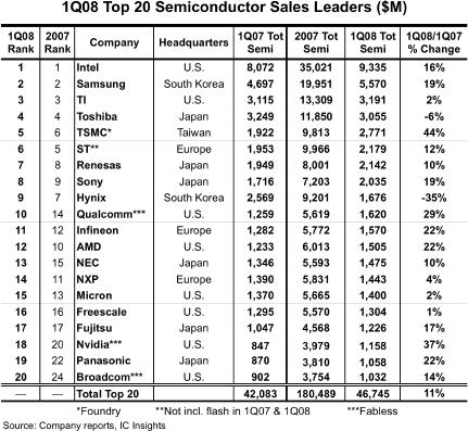 First the movers! Fabless supplier Qualcomm jumped up four spots, ranking as the 10th largest semiconductor supplier in Q1-08. Next, Broadcom, the third largest fabless supplier, also moved up four positions, up to the 20th position. Panasonic (earlier, Matsushita), moved up to the 19th position, while NEC of Japan moved up to the 13th position.
TSMC, the leading foundry, moved up one position, registering the highest — 44 percent — year-over-year Q1-08 growth rate, besides being ranked 5th. Nvidia, the second largest fabless supplier, was another company registering a high YoY growth rate of 37 percent, and moved into the 18th position. Some others like Infineon, Sony and Renesas also climbed a place higher each, respectively. The top four retained their positions — Intel, Samsung, TI and Toshiba.
And now, the shakers! The volatile DRAM and Flash markets have ensured the exit of several well known names such as Qimonda, Elpida, Spansion, Powerchip, Nanya, etc., from the list of the top 20 global semiconductor companies, at least for now.
Among the others in the list, the biggest drops were registered by NXP, which dropped to 14th from 11th last year, and AMD, which dropped two places, from 10th to 12th. Two memory suppliers — Hynix and Micron — also slipped two places, to 9th and 15th places, respectively. STMicroelectronics also slipped from 5th to 6th. IBM too slipped out of the top 20 list.
The top 20 global semiconductor firms comprises of eight US companies (including three fabless suppliers), six Japanese, three European, two South Korean, and one Taiwanese foundry (TSMC). Also, looking at the realities of the foundry market, TSMC’s lead is now unassailable. If TSMC was an IDM, it would be No. 2, challenging Intel and passing Samsung, said one analyst, recently, a thought shared by many.
IC Insights has reported that since the Euro and the Yen are strong against the dollar, this effect will impact global semiconductor market figures when reported in US dollars this year.
There are some other things to watch out for. Following a miserable 2007, the global DRAM module market is likely to rebound gradually in 2008 due to the projected recovery in the overall memory industry, according to an iSuppli report. That remains to be seen.
Some new DRAM camps — such as Elpida-Qimonda, and Micron-Nanya — have been formed. It will be interesting to see how these perform, as will be the performance of ST-backed Numonyx.
Further, the oversupply of NAND Flash worsened in Q1-08, impacted by the effect of the US sub-prime mortgage loan and a slow season, according to DRAMeXchange. The NAND Flash ASP fell about 35 percent compared to Q4-07. Although the overall bit shipment grew about 30 percent compared to Q4-07, the total Q1-08 sales of branded NAND Flash makers fell 15.8 percent QoQ to US$3.24bn. Will the NAND Flash market recover and by when?
