Archive
Cadence integrates chip planning with implementation!
Last month, Cadence Design Systems Inc. unveiled an integrated chip planning and implementation solution. This has been achieved through the integration of Cadence InCyte Chip Estimator and the Cadence Encounter Digital Implementation (EDI) System technologies.
Cadence has called this breakthrough solution, which provides design and implementation engineers with superior visibility and predictability of chip performance, area, power consumption, cost, and time to market across the full range of design activities, including system-level design and IP selection through final implementation and signoff.
I got into a brief conversation with Adam Traidman, Group Marketing Director, Cadence, Dave Desharnais, Product Marketing Group Director, Cadence, and Rahul Arya, Director, Marketing & Technology Sales, Cadence Design Systems India Pvt Ltd.
EDA industry revenue dips 10.7 percent in Q1-09
By the way, the EDA Consortium (EDAC) Market Statistics Service (MSS) today announced that the EDA industry revenue for Q1 2009 declined 10.7 percent to $1192.1 million, compared to $1334.2 million in Q1 2008, driven primarily by an accounting shift at one major EDA company. The four-quarter moving average declined 11.3 percent.
“The business environment remained difficult for EDA as for other industries, with Q1 EDA revenues declining in all regions except Asia Pacific,” said Walden C. Rhines, EDA Consortium chair and Mentor Graphics CEO and chairman. “Nevertheless, for Q1, the overall decline was less than for the previous quarter.”
Back to the current discussion then! It’d be interesting to see how all these tools bring the EDA industry back above the red level!
Why this solution?
The obvious question, why the Integrated Chip Planning and Implementation Solution now?
Adam Traidman said that the Chip Estimator is quite unique! It helps customers early in the IC design cycle.
“We go beyond EDA and estimate cost, etc. We help the designers to do an early architectural level ecomnomical and techical analysis and estimation, etc. Statistics show that during the early phases of design, those decisions can contribute to 80 percent of final design. Today, very few EDA companies provide set of tools and methodologies that allow such trade-off,” he added.
According to him, every customer does this analysis, probably, manually. Cadence is now automating this method. In this respect, it has integrated chip planning with implementation.
“The results of the analysis — you are concerned about accuracy; you look to the EDA vendors to help converge from initial implementation to the actual convergence. Think of it like a cockpit for the design engineer, general manager, program manager, etc.,” he noted.
“You’ve made all the fundamental decisions, etc. If you’re sitting on the physical implementation tool, and you need think through the implications that can be there. For example, to re-synthesize new libraries, etc. We are talking about chip planning at a much, much higher level,” added Traidman.
Helping with IP selection!
The Cadence solution also leverages the vast ecosystem of IP at the ChipEstimate.com portal where over 200 IP suppliers and foundries contribute data. Helping with IP selection has been mentioned among the processes, perhaps, an indicator that designers may have not been able to select the right IPs all this while.
According to Traidman, IP selection and qiuality are key issues. “A lot of people, doing these tradeoffs, could be design managers, general manager, etc. When they sit with this tool, and when it pops up, they can see a huge library of 7,000 IPs from about 200 IP suppliers and foundries. Any design team can view all of the IPs as a free service,” he elaborated. By the way, ChipEstimate is owned by Cadence!
He further added that the ChipEstimate portal allows customers to lower the risks of converging. The portal has been growing since 2006, and receives 1 million page view each month.
Just for interest’s sake, there’s another site — Design And Reuse — that claims to be the world’s largest directory of 8,000 silicon IPs from more than 400 vendors! I have also got into some other discussions — that are ongoing — for developing a similar site in India, for the Indian semiconductor industry!
What about Cadence Encounter?
Post the integration, what happens now to the Cadence Encounter solution and whether it is still available standalone?
Dave Desharnais said the Cadence Encounter solution is still available standalone. “We have integrated some key functions from InCyte. From InCyte, you would normally not have the link to get into physical implementation. Likewise, with feeding back of a fully realized database,” he said.
Last December (2008), Cadence had announced the Encounter Digital Implementation System, a next generation complete RTL-to-GDSII solution for logic and physical implementation.
Along with a fundamental new memory architecture and end-to-end multicore backplane to address the requirements of leapfrog capacity and faster turnaround time for billion transistor designs, it also delivers complete implementation and signoff-in-the-loop for low power, mixed signal, and advanced node design; including the latest 28nm process node where it has been used on over half of the designs being done at this node today.
As per Rahul Arya, since the initial launch, there has been significant usage and endorsement from the world’s largest semiconductor companies, including ST, Toshiba, NEC, NXP, Fujitsu, AMD, and many more that are requested as non-public endorsements.
He added: “The announcement of InCyte and EDI System integration brings a whole new dimension for both system-level and design implementation teams. While both solutions — InCyte and EDI System — are still available as standalone, using both solutions together enables designers at all levels to now have complete visibility into all aspects of the design — from system level architecture requirements and IP selection, to full physical floorplanning, final low power and implementation signoff results.
“The bringing together of both of these solutions delivers literally unprecedented predictability, visibility, and accuracy into all steps of the chip creation and implementation flow for faster design convergence.”
The design solution will be demonstrated at the Design Automation Conference (DAC 2009) in San Francisco this month and made available later this year.
IC Validator offers step up in physical designer's productivity
Recently, Synopsys Inc. introduced an IC Validator design rule checking/layout verification signoff (DRC/LVS) for in-design physical verification and signoff for advanced designs at 45nm and below.
Said to provide a step up in physical designer productivity, it is architected to deliver the high accuracy necessary for leading-edge process nodes, superior scalability for efficient utilization of available hardware, and ease-of-use.
What does IC Validator do?
According to Sanjay Bali, Director of Marketing, Physical Verification & DFM, Synopsys, the IC Validator is a complete physical verification tool, performing increasingly complex DRC and LVS sign-off checks.
It has been specifically architected for in-design physical verification. This means: the place-and-route engineers can run DRC and practical DFM steps alongside place and route within the familiar IC Compiler physical design environment.
And, why need for such a solution? He added that three key summary challenges are driving the need for a new approach and hence the new tool. These are:
a) Increase in complexity and count of manufacturing rules.
b) Unabated growth on design complexity.
c) Increasing DFM challenges, which just cannot be handled in a post processing approach.
Currently, the solution is aimed at 45nm and below as these nodes largely represent the challenges listed above.
Enhancing physical designer’s productivity
Three key tenants of the IC Validator that offer improved physical designer productivity are:
a) High accuracy necessary for leading-edge process nodes.
b) Superior scalability for efficient utilization of available hardware. And,
c) Ease of use with seamless integration of IC Validator and IC Compiler
Bali said: “The IC Validator has been architected from the ground up for in-design physical verification. In-design physical verification enables place-and-route engineers to accelerate the time to tapeout by enabling sign-off quality physical verification from within implementation or physical design. Physical designers designing with IC Compiler can now benefit from the in-design physical verification approach with the push of a button, incurring minimal overhead cost to eliminate surprises late in the design.
“With the verify-as-you-go approach replacing the implement-then-verify approach, physical designers can significantly reduce iteration count, eliminate streamouts and streamins, and accelerate time to tapeout. In addition, the integration enables several productivity enhancing flows like incremental DRC verification, incremental metal fill flows and ECO flows — all leading to significant reduction in time to tapeout.”
It would be interesting to determine or know by approximately what percent is the total physical verification time reduced, and what all does it cover in the process?
Bali added that in extreme cases, finding and fixing DRC violations can easily impact the schedules by a few weeks! The key here is that physical designers typically wait until the final stages of the tapeout to run physical verification. Inevitably, the schedule at this point is squeezed and the cost of fixing the error is high.
“With a sign-off quality physical verification tool integrated into the physical design environment, place-and-route engineers can verify as they implement and eliminate late surprises while speeding up the total physical verification turnaround time. In addition, the outcome of this process is a sign-off clean design.
Production ready!
The Synopsys IC Validator is also said to ‘production ready!” What exactly does that mean?
The IC Validator has been successfully used to tapeout designs at several chip manufacturers, said Bali. In addition, it is currently being used for production designs at Nvidia and Toshiba. Besides other leading foundry’s and chip manufactures it is also qualified by TSMC for 40nm and 28nm process nodes.
For those interested, Toshiba already has Synopsys as its key EDA partner, and NVIDIA adopted the IC Validator for sign-off physical verification, within days of its launch! More are bound to follow!
Saving design spins!
Will the IC Validator approach be able to save design spins? How much is the physical design cycle time reduced?
With the in-design physical verification, place-and-route engineers will be able to run sign-off quality DRC checks, timing aware and sign-off quality metal fill, all within the familiar IC Compiler environment. Linear scalability for efficient use of hardware, sign-off accuracy and integration with IC Compiler will enable productivity enhancing flows like auto detect and autofix, incremental verification flows — all can significantly reduce time to tapeout.
How can it help in avoiding the painful sign-off failure-to-physical-redesign iterations that are increasingly common below 90nm?
With the seamless integration of the IC Validator with the IC Compiler, physical designers can now verify the design as they implement for manufacturing sign-off accuracy.
Incremental DRC’s strength
How good is the incremental design-rule checker (DRC)? Is it really parallelized for the multicore servers?
According to Bali, incremental flows are one of the strongest tenants of IC Validator. To improve physical designer productivity, rule-based only or layer-based only incremental verification runs can be initiated from within IC Compiler.
He said: “For ECO validation, the IC Validator supports window or an area-based incremental verification approach to speed up surgical checks. The incremental flows are meant to be quick, but the IC Validator has multicore capability to further speed up the process.”
The IC Validator discovers and fixes design rule violations within the global context of the design as well. How is this made possible?
With the in-design physical verification, the IC Validator can accurately and automatically identify DRC violation and automatically provide fix guidance to IC Compiler to fix the violation and then re-verify it again.
Handling metal fills and design changes
Operations typically performed during physical verification, such as metal fills, may trigger additional design changes to achieve timing closure. How is this handled by the IC Validator?
Bali said that the prevailing post-processing oriented DFM flows introduce excessive and lengthy discover-fix iterations. Metal fill insertion, a mandatory DFM step at the advanced nodes, exemplifies this issue.
“Physical designers stream out the timing closed post-fill design for signoff validation and then stream it back in to fix any signoff errors flagged during physical verification. This multi-hour discover-fix loop is typically repeated per block till the post-fill design is both signoff qualified and timing clean.
“With in-design physical verification, the IC Validator and IC Compiler address the challenges of DFM, within the place-and-route environment. The seamless integration enables a single pass metal fill flow that is timing aware and of signoff quality and is void of expensive streamouts and streamins,” he added.
New routing tool likely to cover upcoming MCMM challenges: Hanns Windele, Mentor
 This is a continuation of the previous post based on the recent India visit of Hanns Windele, VP Europe and India, Mentor Graphics, where he met key industry figures in a session organized by the India Semiconductor Association. Windele is standing sixth from left, and Poornima Shenoy, president, ISA is standing fifth from right.
Multimode, multicorner tools
Windele mentioned that in every likelihood, another new routing tool would be coming in once the industry enters the 45nm/32nm space. “There is an increasing static timing analysis signoff complexity. The explosive growth in complexity requires multimode and multicorner tools,” he said.
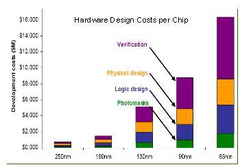
Multicorner and multimode (MCMM) and manufacturing variability will drive the next generation place and route technology. Even in the low-growth markets, technical discontinuities create opportunities for market share changes. For instance, 65nm brings along more than 21 corners/modes scenarios; while 90nm has 10 corners, and 130nm only has four corners.
Therefore, another place and route tool will cover the upcoming MCMM problem. Even in low-growth markets, technical discontinuities create opportunities for market share changes.
 Companies cannot afford the growing cost of EDA. Even the cost of design is growing exponentially, especially, verification, as well as embedded software development costs. Even the EDA revenue has been a flat 2 percent of the IC revenue. However, productivity has been growing as the number of engineers don’t seem to be multiplying in a great way. For example, the transistors produced per electronic engineer has been hearly four-orders of magnitude since 1985.
Showing optimism in recession
Turning to the ongoing recession, which has impacted the semiconductor industry, Windele said that 2009 will be most likely turn out to be the worst recession in the history of the global semiconductor industry.
“It seems to be heading that way. There is also a lot of reason for optimism. I feel that 2009 will be a lot milder than 1985 and 2001,” he said. Even the electronics indsutry’s growth rates have been slowing, decade by decade as well.
Therefore, with this ongoing global recession, why should we remain optimistic? Simple! A crisis translates into opportunities!!
Betting on India
No prizes for guessing where the most opportunities lie — India! Significantly, the ‘middle class’ in urban India becoming a majority. There is likely to be $3 trillion of discretionary spending by 2010. “People who can afford electronic and consumer goods will be growing further,” he added.
Windele cited ISA’s figures, which says that India’s electronics consumption is headed toward $300 billion by 2015. India’s electronic equipment consumption will likely grow at a CAGR of 30 percent through 2015. It was around $28 billion in 2005, and is likely to increase to $127 billion by 2010, and to $363 billion by 2015.
Yet another reason is the growing number of new cell phone subscribers in China and India, which will be 2x larger than the total US subscribers until 2011. Asia is, by far, the most attractive market for new cell phone sales. India will grow fastest, he added.
Downturns compared
Comparing the downturns of the recent years, Windele noted that 2008 and 2009 look different than the other downturns. “There is hardly any inventory left in the industry. One prediction is: as the price upswing comes, prices in the semicon industry will go up very quickly,” he noted.
Seeds already being sown for recovery in 2010. Already, the industry has experiecned two years of severe price declines in memory. Further, systems will be re-designed to take advantage of lower bit prices of FLASH and DRAM.
There will be consolidation and reduced investment in semiconductor capacity in 2008 and 2009. Ramp-up of new system designs will likely happen in 2010 during the period of reduced semiconductor supply.
Concluding, he added that Mentor Graphics became the number 1 EDA company in Europe as the company managed the crisis better than some of our competitors.
State of global semicon industry: Hanns Windele, Mentor
 During his recent trip to India, Hanns Windele, VP Europe and India, Mentor Graphics, took time off to meet key leaders from the Indian semiconductor industry over a session organized by the India Semiconductor Association (Windele is seen here admiring a memento presented by the ISA). He presented his observations of the global semiconductor industry.
According to him, the electronics industry is having a roller coaster ride today. “In the past, it was the same for everyone. Today, it is different! Those who have niche products are doing better than others. The economic crisis is accelerating the downturn in the semiconductor industry,” he added. Windele apprised the audience that the IC unit shipments had fallen 15 percent in Q408 (YoY).
 Windele touched upon the various forecasts presented by various analysts (see chart). The common thing has been — all analysts have forecasted negative growth. The one key stand out has been Future Horizons, which otherwise remains optimistic, but this time forecast a deep negative growth in the industry.
Is the semicon industry really consolidating?
Given the downturn, is the global semiconductor industry really consolidating, as it should? Windele examined some significant revenue and rankings in an attempt to unravel this case. So, do the big keep getting bigger?
As per the semiconductor concentration of revenue, the No. 1 player has had less share in 2007 than in 1972. Applying the same yardstick with the top five companies, they too have had less share in 2007 than they have in 1972! Extending this to the top 10 companies indicated a similar picture!
This goes on to indicate that the global semiconductor industry has actually been “deconsolidating’ since the 1960s! Windele said that between 1965-72, 29 companies entered the market and captured share from the big companies.
Each decade seems to bring in more change. Also, new product families bring new opportunities. Consequently, leadership seems to be changing regularly as well. For instance, 2008 brought the first fabless company — Qualcomm — into the top 10!
Also, new fab-lite strategies are working as well, with companies such as Texas Instruments (TI), STMicroelectronics, Renesas, and Sony among the top 10 as per the H1-08 list.
Based on these assessments, Windele said that few companies have managed to stay on the top for more than three decades. The top 10 seems to be changing every decade, he added. The global semiconductor industry has definitely NOT been consolidating. The top fabs, however, have definitely been consolidating, but not the fabless! “You need to be with the right product at the right time at the right place, otherwise you’d disappear,” he cautioned.
Why hasn’t consolidation happened?
It would be interesting to note why the global semiconductor industry hasn’t been consolidating (yet)! According to Windele, this could be due to:
* Unlike trends in steel, chemicals and automobiles, etc., the electronics industry achieves a reduction in cost per transistor of about 35 percent per year, every year.
* This change enables totally new applications addressing totally new markets.
* These new applications and markets are driven by innovators that are frequently new entrants into the electronics industry.
Opportunities for change
Once the EDA market stabilizes, would there be opportunities for change? There should be plenty of opportunities!
The place and route market has definitely not been growing. Rather, it has been a flat market over the past several years. Nevertheless, new EDA startups lead each new generation of place and route technology. According to Windele, there will be another new routing tool coming in once the industry enters the 45nm/32nm space.
Part II of this post continues in the next blog post.
Synopsys on Discovery 2009, VCS2009 and CustomSIM
 If you’ve been following the EDA industry closely, you’d be well aware of three major announcements by Synopsys over the last couple of days. These are:
* Synopsys introduced the Discovery 2009 verification platform, delivering faster, unified verification solutions.
* It unveiled the VCS multicore technology, delivering 2x verification speed-up.
* It introduced the CustomSim Unified Circuit Simulation solution, which addresses custom digital, analog and memory verification challenges.
 I met up with Dr. Pradip K. Dutta, Corporate Vice President & Managing Director, Synopsys (India) Pvt Ltd and Manoj Gandhi, vice president and general manager, verification group @ Synopsys, in an attempt to understand how significant these announcements are for verification.
Verification is huge!
According to Manoj Gandhi, at the macro level, design complexities continue to grow. As this grows, one big challenge is verification. The reason is: today’s SoC designs and large IC designs, they are being approached like large software projects.
He said: “Verification becomes huge, like software. It is expensive in hardware design. We focus on the verification challenges. We introduced the System Verilog about four to five years ago, and we had also acquired ArchPro. Yesterday, we announced the Discovery 2009, CustomSim and VCS2009.”
How can users make use of new CPUs coming out? “We aim to get higher much performance using multicore architecture,” he added.
Introducing VCS2009
The VCS2009 is multicore enabled, runs the industry’s first low-power verification methodology, and enables fastest mixed-signal simulation with the CustomSIM. Focusing on the VCS2009, Gandhi said: “In verification, there’s a design under test and verification. A lot of designs now have multicores. AMD is among the many folks using the VCS2009. Almost every CPU is designed using VCS. It plays a big role in large SoCs.”
Design companies have several activities such as test bench, debug, etc. All of these can now be parallelized. “Customer designs can be simulated on multiple threads,” Gandhi said. “Also, the applications can also be simulated on different threads, called application level parallelism. We can actually bring about 5-7X improvement in verification with the VCS2009.”
According to him, this product is already being used by some large customers. “This is our next phase of performance innovation. The processor roadmap is getting more and more multicore. We have over 200 customers,” he added.
The VCS distributes time consuming activities across multiple cores. Gandhi added that each core has a lot of computations. You may do lot of parallel activities with the mobile phones. All activities are now in parallel.
And how about the speed-up from parallel computation with the industry-leading Native Testbench (NTB)? He said: “We were one of the first to introduce all technologies as part of a single compiler. That brought the 5X speed-up. We did all of this in verification, and a test bench core was brought into verification.”
The combination of DLP and ALP optimizes VCS performance over multicore CPUs. Design level parallelism (DLP) and application level parallelism (ALP) — all CPUs can be threaded on different cores.
Low-power verification methodology published
Synopsys has published a book on industry’s first low-power verification methodology, along with ARM and Renasas. It is an attempt to bring technology to the mainstream — how to do low-power verification. There are other 30 companies who participated in this exercise.
On the CPF vs. UPF debate, he said that UPF is a standard where Magma, Mentor, Synopsys, etc. have participated. Cadence has CPF. Users can make use of this book and apply, on top of both UPF and CPF.
Introducing Discovery 2009
According to Synopsys, this solution is doing very well in the market. The company has seen strong technology leadership over the last two to three years. It has also created strong investments.
CustomSIM is a unified circuit simulation solution. “We have a software to silicon verification focus. We are all the way from system level design to RTL, to software verification, etc. Discovery has some technologies as part of that, noted Gandhi.
What has Synopsys done right?
A most interesting point in the EDA industry, I feel, has been the performance of Synopsys, in an otherwise difficult segment over the past year. So, what are the reasons behind this success?
Gandhi added: “Our management are all strong technologists. We have invested tremendously in bringing in strong technology leaders. In India, many companies needed R&D collaborations locally. For us, it was a big win when we invested in Bangalore. We work closely with customers delivering technologies that will address challenges two-three years from now.
Dr. Pradip Dutta elaborated: “Synopsys is very strong in product leadership (PL). The other two key areas are customer intimacy (CI) and operational excellence (OE). You need to be highest in PL. We have been very conservative even during strong times.”
That is indeed a marvellous thought! Those who are typically strong in technology, generally go on to develop great intimacy with customers, and all of this starts reflecting on their operations, which are anyway excellent! Here’s a message for those who wish to do well in tough times — strong product leadership, coupled with customer intimacy and well, corresponding operational excellence!
Focus on verification
Now that the focus is quite clearly on verification, how do EVE and the other verification companies stand out? EVE is currently in the emulation space. Gandhi added that EVE competes more wtih Cadence and Mentor. “We work with EVE on many accounts. Verification is all about finding bugs. Emulation has been more cyclical.”
According to him, Synopsys is now looking at tackling the next level — how do you reduce the overall cost? “We will go beyond selling tools. We would look at how to identify issues and saving verification costs.” I believe, verification takes up close to 70 percent of an overall design test.
Commenting on the EDA industry in India, both, Dr. Dutta and Gandhi feel it is still buzzing quite well, despite what’s been happening in the global context. “We have invested quite a lot. We have a large team here. We continue to collaborate with local institutions here as well,” Dr. Dutta added.
Cadence's Encounter and how it matches up to Synopsys' Galaxy!
Early December 2008, Cadence Design Systems launched the Cadence Encounter Digital Implementation System, said to be a configurable digital implementation platform that delivers an incredible scalability with complete support for parallel processing across the design flow. Will it change the fortunes of the struggling EDA industry? EDA industry stats for Q3-08 given at the end of this post!
My first thoughts immediately went to Synopsys’ Galaxy Custom Designer solution. This is the industry’s first modern-era mixed-signal implementation solution. Is the Cadence Encounter an answer to Synopsys’ Galaxy? This is worth a shot!
 Obviously, why has Cadence released Encounter now? How will the Encounter take on Synopsys’ Galaxy? I managed to engage Rahul Deokar, Product Marketing Director, Cadence, to find out more.
The Encounter Digital Implementation System is a next generation high-performance, high-capacity RTL-GDS-II design closure solution with the industry’s first end-to-end parallel processing flow that enables all steps of the design flow to be multi-CPU enabled — from floorplanning, placement, routing, extraction to timing and signal integrity sign-off. He said, “At its core is a new memory management architecture and end to end multi-CPU backplane that provides scalability with increased performance and capacity to reduce design time and time-to-market.”
Does it intend to take on Synopsys’ Galaxy? Well, Deokar said: “Yes, it surpasses the other solutions available in the marketplace based on the following capabilities and features, which are:
* Ultra-scalable RTL-to-GDS-II system with superior design closure and signoff analysis for low-power, mixed-signal, advanced node designs.
* End-to-end multi-core infrastructure and advanced memory architecture for unparalleled scalability of capacity, design turnaround time, and throughput.
* Robust design exploration and automated floorplan synthesis and ranking solution.
* Embedded signoff-qualified variation analysis and optimization across design flow.
* Integrated diagnostic tools for rapid global timing, clock and power analysis/debug
Here’s a list of benefits that it provides designers:
* Significantly reduces design time, schedule and development risk.
* Increased productivity through automation; superior quality of results.
* Configurable and extensible platform that ensures maximum utilization and ROI — upgrades proven design flow and amplifies existing expertise.
* Interoperability across package, logic, custom IC design, and manufacturability.
Harnessing power of multicore computing
According to Cadence, it provides complete support for parallel processing across the design flow. Does this mean that designers can fully harness the power of multicore computing? It would also mean that today’s EDA tools capable enough to meet the multi-core challenge.
Deokar added: “Yes, the end-to-end parallel processing flow is supported across the entire design flow and consequently. Also, designers can fully harness the power of multicore computing. Today’s designers commonly have dual CPU or even quad CPU machines on their desktop. The Encounter Digital Implementation System allows the designers to leverage their multi-CPU hardware and gain significant TAT improvements on the design cycle time and overall development schedule.”
The Encounter end-to-end multi-CPU backplane delivers ultra-scale performance gains up to 16X in key areas such as routing and timing closure. All steps of the design flow are multi-CPU enabled. For instance, on a production design, when the Encounter is run on four CPUs, the user can get a 3.2X performance boost across the entire, end-to-end design flow.
Encounter deployed by over 15 customers?
Designers are said to be reporting dramatically improved design time, design closure, and faster time-to-market for advanced digital and mixed-signal devices. By what factors, and against which other tool(s) has Encounter been rated?
Deokar said that the Encounter Digital Implementation System has been developed in close collaboration with over 15 customer partners who have extensively used, validated and now, deployed it.
“Customers are already seeing overall design cycles significantly shorted by 25-30 percent, which translates to multiple weeks or even months. These significant improvements are against competitive tool flows in their current methodology,” he added.
Encounter is also said to be offering new technologies for silicon virtual prototyping, die-size exploration and RTL and physical synthesis, providing improved predictability and optimization in early stages of the design flow.
Regarding this aspect, he pointed out that large scale design complexities (increased functionality, predictability, productivity, etc.,) pose some of the biggest challenges. Designs are getting huge at 100M+ gates, 100+ macros in the design, putting significant requirements on design tools, particularly, floorplanning of these macros, and the whole design becomes a huge challenge.
“The new Silicon Virtual Prototyping capabilities of Automated Floorplan Synthesis and Die Size Exploration help out exactly on that front. These can quickly provide floorplanning for that large 100M+ gates, 100+ macro design.
“And not just one floorplan, but designers can provide multiple criteria (say, along the lines of timing or power or area or congestion) and you will get multiple floorplans with their rankings…– all this in a matter of minutes! Essentially, you could finish your breakfast or lunch (depending upon how fast you eat!) and be back to have multiple floorplans that you can then pick and choose from, and then proceed to implementation.”
Addressing new problems at 45nm/40nm/32nm
Obviously, targeted at 45nm/40nm/32nm, etc., how can or how does Encounter anticipate and address the majority of the new problems associated with these geometries across the entire flow?
Deokar noted that its main customers include semiconductor companies working on 45nm and 32nm designs, with aggressive design specifications including 100 million or more instances, 1,000-plus macros, operating speeds exceeding 1GHz, ultra-low power budgets, and large amounts of mixed-signal content.
“The challenges facing these designs comprise of an increasing demand for design tool performance/capacity and design features for challenging ultra-large scale designs in the areas of low power, mixed signal, advanced node and signoff analysis. In addition, small market windows and product life-cycles and the cost pressures further exacerbate the situation,” he noted.
The Encounter Digital Implementation System’s core design closure capabilities, plus the new advanced node technologies, including litho-, CMP-, thermal, and statistical-aware optimization provide comprehensive manufacturing- and variation-aware implementation, and an end-to-end multi-core infrastructure for fast, predictable design closure even on the most challenging designs.
Reducing memory footprints
It will be interesting to learn about the kind of work that has gone into reducing the memory footprint of the most memory-retentive applications.
Deokar said that an innovative memory architecture is at the core of the Encounter System that enables capacity and performance gains of 30-40 percent for full flat and hierarchical designs, even if you are running on a single-CPU machine.
Cadence’s R&D team has developed an advanced memory defragmentation algor
ithm that allows the applications to be extremely memory-frugal …and that memory-efficiency enables designers to handle their biggest 100M+ instance designs.
Parallels with Synopsys’ Galaxy Custom Designer?
There seem to be parallels with Synopsys’ Galaxy Custom Designer for AMS. Also, there could be some chance of Cadence’s Virtuoso and Encounter coming together in future.
According to Deokar, Synopsys’ Custom Designer for AMS is its entry into the full-custom/analog design marketplace, where the Cadence Virtuoso platform is a strong incumbent.
He said: “The biggest challenge for mixed signal designers is the efforts/resources involved in taking design data from the full-custom/analog tools to the digital implementation tools, and back and forth…in never-ending iterations.
“Now, with the Encounter Digital Implementation System, designers get the seamless full-custom/analog and digital design implementation interoperability…with unified constraints handling, mixed-signal floorplanning and ECO. It executes off a common design database (OpenAccess), enabling edits made in one design environment (e.g. Virtuoso) to be easily seen in the other design environment (e.g. Encounter). It also enables the design team to easily transfer the design data, to determine the optimal floorplan based on analog and digital constraints.”
For example, the analog design team moves pins on the analog block, when the design is opened in Encounter, the modified pin locations are easily seen and the digital design team can execute a pin optimization to re-align the pins at the top-level.
In addition, the user can enter routing constraints in either Encounter or Virtuoso, and implement mixed signal routing in either environment. Top-level routing constraints could be defined within Virtuoso, then the top-level routing completed using the mixed signal routing functionality within Encounter.
Customers are already seeing their overall design schedules significantly reduced, added Deokar.
Postscript: Well, as expected, the EDA industry has taken a hit again. As per the EDA Consortium (EDAC) Market Statistics Service (MSS), the EDA industry revenue for Q3 2008 declined 10.9 percent to $1,258.6 million compared to $1,412.1 million in Q3 2007. The four-quarter moving average declined 2.8 percent.
Now, does Cadence’s Encounter have the ability to turn around the EDA industry’s fortunes? I don’t think so! Much more needs to be done by Cadence and all of the other EDA companies!
Rapidly growing local market bring new opportunities for EDA in India
Those following the EDA industry are well aware that its been an industry in some trouble right through this year.
If you visited EDA Consortium’s web site, this becomes clear. In Q1-08, the global EDA industry revenue for Q1 2008 declined 1.2 percent to $1,350.7 million compared to $1,366.8 million in Q1 2007.
Later, the EDA industry revenue for Q2 2008 declined 3.7 percent to $1357.4 million compared to $1408.8 million in Q2 2007, as reported by the EDA Consortium.
I am still waiting to see how the Q3 results shape up. My guess is, it would be even lower than Q2, unless there are a few surprises!
The EDA market in India, as per the ISA F&S Report 2005, was US$110m. The latest figures are not yet available, though I would believe the Indian EDA industry is likely to do better than the global industry, unless, there have been some slowdown effects here as well.
 I had an interesting discussion with Jaswinder Ahuja, Corporate Vice President and Managing Director, Cadence Design Systems (I) Pvt. Ltd and Chairman, India Semiconductor Association (ISA), on the (dipping?) fortunes of the EDA industry lately.
According to Ahuja, 2008 has been a challenging year. The global financial crisis has impacted several industries and the EDA industry was no exception. Due to the overall downturn in the economy, companies are being more cautious and are delaying purchase decisions, a move that is impacting the overall EDA industry.
Coming to the drivers for EDA in India this year, there are a few key ones! First, the design centres have gained expertise and are now doing cutting-edge designs out of India. They have moved up the value chain from doing block-level design to increasingly owning up end-to-end design and design starts.
Second, several Indian design services companies have made significant acquisitions, showing that their businesses have not just taken root, but also flourished. MindTree Consulting’s acquisition of TES PV and Wipro’s acquisition of Oki’s wireless chip design arm are cases in point, added Ahuja.
He said: “The Indian EDA industry has been growing and we will see more technology adoptions and proliferations in India Design Centers. Also, the rapidly growing local market is unfolding new opportunities.”
EDA outlook 2009
Going forward, market pressures and design complexities are just some of the issues design teams face today. Cadence’s customers, for instance, would like to plan in the context of IP selection, run analysis around power, performance and cost perspectives. Design predictability will be a priority, said Ahuja.
The key focus areas for the EDA industry will be new design for manufacturing technologies as designs move to advanced nodes; verification and verification IPs and multicore processing support for EDA flows as a result of increased integration.
Also, SaaS is likely to gain traction as companies are compelled to consider flexible engagement models to access state-of-the art design environments that help design teams reduce risk and cost, yet increase time-to-productivity.
Are there any opportunities for EDA folks in solar? Ahuja disclosed that in a recent poll by ISA, to the question ‘Solar PV has potential in India’, almost 90 percent of respondents replied Agree or Strongly Agree.
With the worldwide focus on alternative energy systems, India has witnessed several companies announcing investments in PV segment. This is good news for the Indian semiconductor ecosystem.
Cadence has a broad portfolio of technologies that addresses the needs of different players in the ecosystem.
Low power initiatives
Low power has always been a key focus area in semiconductors. According to Ahuja, power efficient design is gaining importance across the design chain and EDA companies will have to look closely at ‘green’ technologies.
Energy efficiency at the system and application level for wired and wireless products will be one of the focus areas. Emerging technologies that allow applications and systems developers to evaluate how their programs use power both individually and in a dynamic, multi-application model of the end system will help expand the role of EDA into system-level design.
The Power Forward Initiative (PFI), an industry alliance comprising of companies across the semiconductor design chain will work towards a more systematic, integrated approach to low-power design.
Outlook 2009
With the new year about to start in less than a week’s time, the impact of the financial crisis will see an increased demand for mid-range product technology as consumers shift spend toward ‘essential’, rather than ‘desirable’ electronic products.
As per Ahuja, globally, semiconductor companies are focusing on their core strengths, consolidating and realigning resources. Across sectors, they will look for systems that marry functionality with cost efficiencies.
“Growth for semiconductor companies will come from energy related and low-power technologies that are able to drive market share shifts,” he noted.
Cadence's Virtuoso vs. Synopsys' Galaxy Custom Designer!
Synopsys recently introduced the Galaxy Custom Designer, which provides a unified solution for custom and digital designs, thereby enhancing designer efficiency.
Well, this solution invariably draws a comparison with Cadence’s Virtuoso platform within the EDA industry!
 That prompted me to engage Sandeep Mehndiratta, Product Marketing Group Director, Cadence Design Systems, in this discussion. We discussed a range of issues, such as how the Synopsys’ Galaxy Custom Designer matches up with the Virtuoso, and whether designers can now design what they wish, including concepts and flows, as well as the relevance of open architectures.
For the record, a few years ago, Cadence introduced the next-generation Virtuoso custom design IC 6.1 platform, which had a major upgrade recently with the IC 6.1.3 release. This release has been production-proven with tapeouts from many customers. However, as I said, it is Synopsys’ Galaxy Custom Designer doing the rounds in the EDA circles as of now!
Galaxy Custom Designer vs. Virtuoso
It is well known that Cadence has been the established leader in custom IC design space for decades, and has been constantly improving and upgrading technology to ensure it is providing best-in-class platform for designing today’s complex custom chips.
Mehndiratta said: “A couple of years ago we introduced the next-generation Virtuoso custom design IC 6.1 platform. This release has been production-proven with tapeouts from many customers. Some of the leading customers that have adopted the Virtuoso platform include Ricoh, National Semiconductor, Cambridge Analog Technologies Inc., Matsushita, etc.
“Synopsys has recently launched Galaxy Designer and it is unproven as yet. From what we’ve read and heard from some of our mutual customers, the competitive introduction may be attempting to replicate older custom IC technology. While the jury will probably be out for some time on this unproven tool, Cadence continues to provide a complete solution for design, verification and implementation of complex analog and mixed-signal designs, differentiated by the tight integration between the underlying technologies.”
With the advent of Galaxy, is it now safe to say that designers can finally design what they wish, including concepts and flows? Well, the answer’s not yet there! However, Mehndiratta did touch upon Cadence’s solution that is built upon decades of experience in this area and a strong eco-system made up of partners, third-party providers and foundries. Virtuoso, he added, is the most complete eco-system for designing ICs; not only with its inherent flow, but also because of its linkages to multiple tools inside and outside of Cadence.
“For many years, we have provided a consistent front-to-back flow, and over that time we have learned much about what customers need to do their designs efficiently. It is that knowledge base that we leveraged to accelerate productivity with 6.1 release couple of years back,” he added.
If that is the case, why has it taken so long for a first modern-era mixed-signal implementation solution to be in place?
He referred to Cadence’s next generation Virtuoso 6.1 introduced in November 2006, said to be the first modern, and most complete custom design solution released natively on the OA database. Productivity benefits are significant. RFIC Solutions Inc., a third-party intellectual property and design service provider, is said to have increased productivity two-fold by adopting the Cadence Virtuoso custom design platform.
Likewise, INSIDE Contactless, a fabless company and leader in contactless technology providing high-performance chipsets for secure, fast and reliable transactions with electronic identification, saved 20 percent in development time by adopting Cadence Virtuoso UltraSim Full-Chip Simulator, a component of Virtuoso Multi-Mode Simulation with a high-performance digital-solver technology, for the verification of its current and next-generation contactless and Near Field Communication (NFC) system-on-chip (SoC) designs.
He noted: “Specifically, mixed-signal design is evolutionary, not revolutionary. The concept of mixed-signal design isn’t new. People have been designing in this manner for 15+ years. What is new is the more holistic approach being taken by designers developing mixed-signal circuits. The once clear lines between analog and digital design are blurring, and now the idea of “mixed-signal” is being architected in right from the beginning.
“That is why Cadence’s AMS Designer covers transistor to system level design with a single simulation solution for complete verification. It is why Cadence has combined the power of its leading implementation platforms (Virtuoso and Encounter) to handle the implementation of mixed-signal designs.”
Given that Synopsys’ Galaxy Custom Designer can provide a unified solution for custom and digital designs, thereby enhancing designer efficiency, how will it change/affect designing, and the EDA landscape?
Mehndiratta pointed out that Cadence had defined a unified solution long ago. “Our industry leadership in this area, and Synopsys mimicking of that solution are testaments of Cadence’s vision. Competition is good for all industries, the end-customer usually benefits. You can count on Cadence to not only remain competitive, but also retain our industry leadership in custom/mixed-signal design.”
Importance of open architecture
Let us also look at the importance of open architecture that natively supports interoperable PDKs.
Cadence also believes in open architectures. Its Design Framework II was built as an open architecture, and that’s the reason, why there are many companies that have connected (30+) to form a larger ecosystem. Whereas, the Industry Standard Framework has been tried and failed, the company maintains.
Mehndiratta said: The reason it was a failure is the same as interoperable PDKs. Building frameworks and PDKs that are based on a “lowest common denominator” principle do not provide the most optimized design flow. Instead, you are left with systems that try to please everyone and in the end are rejected as bloated beasts retarding the progress of design.”
Finally, how does Cadence propose to address the Galaxy challenge?
As expected, Cadence hopes to continue to provide customers and partners with a framework in which they can build their tools into the Virtuoso design flow in the most optimized way possible.
Also, by providing its proven and industry standard Pcell technology that takes advantage of the key features in Cadence’s design flow, thereby allowing for fast and productive design today and in the future.
Synopsys' Galaxy Custom Designer tackles analog mixed signal (AMS) challenges
Synopsys Inc. recently unveiled its Galaxy Custom Designer solution, the industry’s first modern-era mixed-signal implementation solution. Architected for productivity, the Galaxy Custom Designer leverages Synopsys’ Galaxy Design Platform to provide a unified solution for custom and digital designs, thereby enhancing designer efficiency.
 Galaxy Custom Designer delivers a familiar user interface while integrating a common use model for simulation, analysis, parasitic extraction and physical verification. It is the first-ever implementation solution built natively on the OpenAccess database for legacy designs as well as a new componentized infrastructure offering unprecedented openness and interoperability with process design kits (PDKs) from leading foundries.
Subhash Bal, Country Director, Synopsys (India) EDA Software Pvt. Ltd, highlighted three key features: One, it is architected for productivity. Two, it is a complete custom design solution. And three, it is based on an open environment.
The key question: why the Galaxy Custom Designer, and why now? Simple! The modern AMS era is characterized by interdependent custom and digital functions; analog IP is now mainstream; and there is the phenomena of an increased embedded memory. Current solutions are said to possess limited horizon. Hence, Galaxy!
A new solution is said to be the need of the hour, which is complete — verification and implementation, with common models, extraction, analysis. Re-spin is not an option. Next, unified implementation, which addresses both custom and cell based needs. Custom and cell based functions are highly interdependent. Also, close to 100 percent of designs today are AMS.
Finally, the solution has to be open and portable. This accelerates the design cycle and IP portability. Also, quicker access to process details is a must! Architected for productivity, Galaxy Custom Designer has a similar look and feel, and works using fewer clicks — three as against six!
Galaxy Custom Designer’s Schematic Editor has productivity enhancers such as real-time connectivity, on-canvas editing and smart connect. Similarly, productivity enhancers for its Layout Editor include push button DRC and Extract, standard TCL and Python PCells, and auto via and guard ring generation. The WaveView Analyzer has features such as highest capacity and performance, complex analysis toolbox, and an automated TCL verification scripting.
A unified platform for cell and custom means superior ease of use, performance, capacity and data integrity. Open and portable, it facilitates plug-and-Play IP as well as standards based PDK, which means one PDK for all tools, added Synopsys’ Bal.
The IPL (Interoperable PDK Libraries) is an industry alliance established on April 2007 to collaborate on the creation and promotion of interoperable process design kit (PDK) standards.
Wipro Technologies has been among the early users of the Galaxy Custom Designer. I also managed to speak with Anand Valavi, Group Head, Analog Mixed-Signal Group, Wipro Technologies.
Valavi said: “From an EDA tool perspective, in AMS area, the amount of productivity is a lot less than in the digital area. The per transistor productivity for a digital designer is several magnitudes higher than an analog designer.”
The methodology is definitely not as evolved as in the digital area. According to him, ‘This productivity will now increase for analog and AMS areas, and people can do a lot more complex designs in a shorter period of time. There has been a lot of integration.”
On the salient features or enhancements, he said there have been reasonably good improvement in several areas. One, there is an alternative, now, and that brings a lot of advantages. Two, when you take it down to next level, there are several other technical reasons.
Valavi added that an integrated environment definitely improved the productivity. There are other minor things. When you start using it, there are things that helps technical users — for example, an on-canvas editing. Also, the usage or collaborative results in the iPDK libraries will improve the effectiveness in chips designs that are churned out. “It will surely give people working in analog design area a choice,” he noted.
Mentor Graphics: DFM is where all the value is!
 As promised, here is the concluding part of my discussion with Joseph Sawicki, vice president & GM, Design to Silicon Division, Mentor Graphics.
We went over the design for manufacturing (DFM) challenges and how yield can be improved. He also touched upon the design challenges in 45nm and 32nm, respectively.
Given that the semiconductor industry does speak a lot about DFM, what steps are being taken to improve on the overall yield?
According to Sawicki, in the VLSI microchip era, yields started at 60-70 percent, and so DFM wasn’t required. However, in the nanochip era, DFM is where all the value is. [VLSI Research.]
Joseph Sawicki, vice president & GM, Design to Silicon Division, Mentor GraphicsHe added that at smaller geometries, manufacturing variability has a much greater impact on timing, power dissipation, and signal integrity. Traditional guardbanding is no longer sufficient to guarantee competitive performance at acceptable yields, and excessive design margins erase the advantages sought by going to the next node in the first place.
Moving to advanced technologies without dealing effectively with manufacturing variability can actually put a design at a competitive disadvantage due to low parametric yield.
“Successful IC implementation requires a detailed understanding of how variability affects both functional and parametric yield. Customers need a manufacturing-aware engineering approach that extends across the entire physical implementation life cycle, starting with cell library development and extending through place and route, physical verification, layout optimization, mask preparation, testing, and failure analysis.
“They need a design flow that helps them “co-optimize” for both performance and yield simultaneously, based on accurate models of manufacturing process variability. The ability to do this quickly and effectively can give IC designers a powerful competitive advantage,” Sawicki said.
There is no silver bullet! It takes a broad-based, well-integrated approach to have a significant and consistent impact on manufacturability.
According to him, Mentor Graphics provides a complete manufacturing-aware design-to-silicon solution addressing random particle effects, small-scale device and interconnect interactions, lithographic distortions and process window variations, and thickness variations resulting from chemical-mechanical polishing (CMP) and variable film deposition and etch rates.
“Our tools incorporate comprehensive, highly-accurate models that have been tuned and verified for specific manufacturing environments, and address every stage of the digital IC implementation life cycle,” he added.
So, how is Mentor handling 45nm and 32nm design challenges?
Sawicki added: “Advanced process nodes present challenges at every stage of IC implementation, from place-and-route, through physical verification, layout enhancement, testing and yield analysis. Mentor has a complete design-to-silicon flow that addresses the critical challenges of IC implementation at every stage.”
