Archive
Identifying growth opportunities in PV materials market
SEMI USA had a session on “Identify Growth Opportunities in the PV Materials Market,” which was presented by Mike Corbett, Linx-AEI Consulting, and moderated by Bettina Weiss of the SEMI PV Group.
More, in a short while! 😉 Stay tuned!
Will solar downturn lead to more mature PV industry?
The severe downturn in the global Photovoltaic (PV) market in 2009 actually could have a positive outcome for the worldwide solar industry, yielding a more mature and orderly supply chain when growth returns, according to iSuppli Corp.
Worldwide installations of PV systems will decline to 3.5 Gigawatts (GW) in 2009, down 32 percent from 5.2GW in 2008. With the average price per solar watt declining by 12 percent in 2009, global revenue generated by PV system installations will plunge by 40.2 percent to $18.2 billion, down from $30.5 billion in 2008.
The figures present iSuppli’s forecasts of global PV installations in terms of gigawatts and revenue.
Fig 1: Global Photovoltaic System Installation Forecast in Megawatts, 2008-2013 Source: iSuppli, April 2009
“For years, the PV industry enjoyed vigorous double-digit annual growth in the 40 percent range, spurring a wild-west mentality among market participants,” said Dr. Henning Wicht, senior director and principal analyst for iSuppli. “An ever-rising flood of market participants attempted to capitalize on this growth, all hoping to claim a 10 percent share of market revenue by throwing more production capacity into the market. This overproduction situation, along with a decline in demand, will lead to the sharp, unprecedented fall in PV industry revenue in 2009.”
However, the 2009 PV downturn, like the PC shakeout of the mid 1980s, is likely to change the current market paradigm, cutting down on industry excesses and leading to a more mature market in 2010 and beyond.
Fig 2: Global Revenues Generated by Photovoltaic Installations 2008-2013 in Millions of US Dollars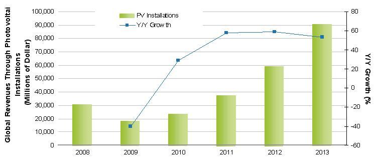 Source: iSuppli, April 2009
“The number of new suppliers entering and competing in the PV supply chain will decelerate and the rate of new capacity additions will slow, bringing a better balance between supply and demand in the future,” Wicht said.
Blame it on Spain
The single event most responsible for the 2009 PV market slowdown was a sharp decline in expected PV installations in Spain. Spain accounted for 50 percent of worldwide installations in 2008. An artificial demand surge had been created in Spain as the time approached when the country’s feed-in-tariff rate was set to drop and a new cap of 500 Megawatts (MW) loomed for projects qualifying for the above-market tariff. This set a well-defined deadline for growth in the Spanish market in 2009 and 2010.
While the Spanish situation is spurring a surge in excess inventory and falling prices for solar cells and systems, this will not stimulate sufficient demand to compensate for the lost sales in 2009. Even new and upgraded incentives for solar installations from nations including the United States and Japan—and attractive investment conditions in France, Italy, the Czech Republic, Greece and other countries—cannot compensate for the Spanish whiplash in 2009.
The Spanish impact will continue into 2010, restraining global revenue growth to 29.2 percent for the year. Beyond Spain, the PV market is being adversely impacted by the credit crunch.
“Power production investors and commercial entities are at least partially dependent upon debt financing,” Wicht noted. “Starting in the first quarter of 2009, many large and medium solar-installation projects went on hold as they awaited a thaw in bank credit flows.”
After the fall
After 2010, the fundamental drivers of PV demand will reassert themselves, bringing a 57.8 percent increase in revenue in 2011 and similar growth rates in 2012 and 2013.
“PV remains attractive because it continues to demonstrate a favorable Return on Investment (RoI),” Wicht said. “Furthermore, government incentives in the form of above-market feed-in-tariffs and tax breaks will remain in place, making the RoI equations viable through 2012. Cost reductions will lead to attractive RoI and payback periods even without governmental help after 2012.”
Furthermore, lower system prices will open up new markets by lowering incentives and subvention costs. The lower the PV system prices are, the lower the incentives will have to be. Developing regions will be big the beneficiaries of these lower prices and thus will grow faster than the global average, Wicht said.
Source: iSuppli, USA
Solar sunburn likely in 2009? India, are you listening?
iSuppli’s just issued a warning that 2009 could well see the coming of a solar market eclipse!
Come to think of it! Just last week, in the Semiconductor International webcast, the analysts did mention that there could be tough times ahead for solar! In fact, Aida Jebens, Senior Economist, VLSI Research Inc., did indicate that solar/PV would pick up in the next two years and that 2009 could be a tough year.
If you look at the India situation, I have been getting the feeling all the time that all of a sudden, too many companies were entering this market segment, as though it is a land of promised gold! Perhaps, it is, and one sincerely wishes that all of those investments proposed for solar do not come unstuck.
This August, following the announcement of the national semiconductor policy (the Special Incentive Package Scheme, or SIPS), the government of India received 12 proposals amounting to a total investment of Rs. 92,915.38 crore. Ten of these proposals were for solar/PV, from: KSK Surya (Rs. 3,211 crore), Lanco Solar (Rs. 12,938 crore), PV Technologies India (Rs. 6,000 crore), Phoenix Solar India (Rs.1,200 crore), Reliance Industries (Rs.11,631 crore), Signet Solar (Rs. 9,672 crore), Solar Semiconductor (Rs.11,821 crore), TF Solar Power (Rs. 2,348 crore), Tata BP Solar India (Rs. 1,692.80 crore), and Titan Energy System (Rs. 5,880.58 crore).
Then, late September, Vavasi Telegence (Rs. 39,000 crore), EPV Solar (Rs. 4,000 crore), and Lanco Solar (Rs. 12,938 crore), also announced major investments.
Now, given the quite ruthless kind of financial crisis the world is currently engulfed in, several have raised doubts whether solar players would be able to get the credit they need. Or, would they run into rough weather?
On paper, some of these companies are big corporate houses, with several years of standing. However, reality can be quite different, and can bite! I’ve yet to hear whether all of these companies have managed to raise the requisite capital. One sure wishes that they have all been busy and will be successful!
Otherwise, all one needs to look at is iSuppli’s warning. According to iSuppli, ‘Bringing an end to eight consecutive years of growth, global revenue for photovoltaic (PV), panels is expected to plunge by nearly 20 percent in 2009, as a massive oversupply causes prices to drop.’
Will it be a case of massive oversupply in India? We haven’t exactly started. Hence, perhaps, we will come to deal with oversupply later. The key thing is to get all of these solar/PV projects off the ground!
The India Semiconductor Association (ISA), and now, SEMI India, have been promoting the solar/PV industry very aggressively. The work they’ve done so far has been commendable, and I’ve been witness to all of their activities. However, keep in mind that these are only industry associations, who can only advice, guide, debate and promote the industry, and also provide industry statistics for everyone to consume.
The real action can only happen once the proposals have been cleared by the Indian government and the players have managed to arrange for the requisite capital for their projects. The Indian fab story with SemIndia is all to familiar, and there should not be a repitition with solar/PV projects.
Therefore, the role of the government of India will be extremely critical and crucial. The good health of the Indian solar/PV industry is entirely in its hands, and not in the hands of the industry associations.
Perhaps, the Indian government could do well to look at how the Taiwan government is playing a critical role in reviving the hard hit DRAM industry and also at the German free state of Saxony, which has played a key role in financing the ailing Qimonda.
Otherwise, the Indian solar/PV industry could get hit, even before it takes off the ground! And, as a nation, we cannot afford that to happen!
India has so far has had a good story going in solar. There are hopes that solar/PV will trigger off a spate of manufacturing activities in India, besides creating lots of jobs. Don’t think we can afford to spoil all of this!
The industry in India is still very much in its infancy. Let the baby play happily in the water (solar) tub, instead of throwing the water out! This baby needs a lot of hand-holding to get stronger in the years to come.
Practical to take solar/PV route: Dr. Atre, Applied
 Solar/PV is perhaps, a practical route for India to enter manufacturing, contends Dr. Madhusudan V. Atre, president, Applied Materials India. Alternatively, another way to enter this field could be by having solar farms.
According to Dr. Atre, India has a strong potential for manufacturing. The Indian scenario has the talent pool and an emerging middle class, along with the presence of system design and chip design companies. Only a fab seems to be the missing piece from this ecosystem!
Benefits of a fab include: fuels economic productivity, contributes to GDP and adds to national growth, creates jobs, helps set up the other expertise necessary for an ecosystem, and closes the loop between market, design, manufacture, test, customer.
Indian fab scenario
Commenting on the Indian scenario, Dr. Atre, says: “For PV, about $200-500mn is needed for a fab. If we can enter into manufacturing via the solar/PV route, the scale of investment required would be much less [than the investment needed for a wafer IC fab]. This can be practical route to enter manufacturing in India, and less complexity is involved, as compared to an IC fab.” Another way of entering manufacturing is by having solar farms.
Applied’s external face in India involves: Take leadership role in industry bodies; work with the government on various semiconductor and manufacturing policies; look for potential investments in start-ups; work with the academia on collaborative research in nanomanufacturing; be sponsors in key conferences; drive corporate social responsibility programs; and help enable semiconductor and solar manufacturing in India.
Touching on some emerging areas of interest, Dr. Atre highlights that packaging is very important in semiconductors. “We may look at some company in packaging R&D. We have invested a bit in Tessolve,” he says. “We would also like to see the success of the nanotech lab in IIT-Mumbai, and see how it can help India.” On a global scale, he notes that Applied would be setting up two-three SunFab lines with Masdar in Abu Dhabi, UAE.
Applied Materials in India
Headquartered in Bangalore, Applied has been present in the country for over five years. It has approximately 1,500 employees and associates. A liaison office was originally set up in May 2002. Applied Materials India Pvt Ltd (AMIPL) was set up in July 2003, and operations started in November 2003 with cost + model. It consolidated all Applied operations in Bangalore into ITPL (~92,000sqft). It also merged Brooks Chennai (~100RFTs) into Applied India operations. Applied currently has R&D centers in Bangalore and Chennai.
Next, Applied established site operations in Delhi (~5000 sqft) to support Moser Baer. Its key partners are Satyam, Wipro and TCS, on various aspects of engineering and software services. In Delhi, Applied has 25-30 people to support Moser Baer, where it has the first SunFab line up and running.
In Mumbai, it has set up a nanomanufacturing lab with IIT-Mumbai. “We have put in equipment worth $7-8 million there, and do R&D projects,” adds Dr. Atre. The nano lab at IIT-Mumbai was inaugurated in November 2007 by Mike Splinter, president and CEO, Applied Materials.
Applied is also involved in the potential upgrade of SCL. “We are working with some other companies on how we can upgrade SCL. We are more at the backend to set up some capabilities,” he says.
Applied Ventures makes investment in emerging technologies and companies. It has funded a couple of companies in the semi start-up stage. Applied Ventures looks at global investments.
Moser Baer is Applied’s first customer in India. It has a 35-40MW assembly line. This is the first time that 5+m2 solar panels will be coming out. The panel will now have to be taken up to the production ramp. Dr. Atre adds that Europe was much advanced in solar/PV. Germany, especially, was far advanced in the implementation aspect, as well as Italy and Spain.
Nanomanufacturing simplified
Nannomanufacturing, as per Wikipedia, is “the near-term industrial-scale manufacture of nanotechnology-based objects, with emphasis on low cost and reliability.” To manufacture at this level requires a lot of expertise, skills, etc., says Dr. Atre. Cost is definitely an important driver, and so is reliability, he adds. According to him, nanomanufacturing technology combines the two core strengths of Applied: nano + manufacturing.
Applied’s vision has been to apply nanomanufacturing technology to improve the way people live. Its mission: To lead the Nanomanufacturing technology revolution with innovations that transform markets, create opportunities, and offer a cleaner, brighter future to people around the world.
Applied Materials is a global leader in nanomanufacturing technology solutions with a broad portfolio of innovative equipment, service and software products for fabrication of: semiconductor chips, flat panel displays (using TFTs), solar photovoltaic cells and modules (in crystalline and thin film vectors), flexible electronics, and energy efficient glass (BIPV). The last three categories fall under EE or the Environment and Energy Division.
Dr. Atre says: “We have the SunFab line for solar/PV. In flexible electronics, as an example, you can have solar cells wrapped around an object.” As for energy-efficient glass, you can save on AC costs, etc., by using building integrated photovoltaics.
Core capabilities
Applied’s core capabilities include: commercialize sophisticated systems and thin-film engineering, besides a global culture. “Our technological strengths include semiconductors, solar/PV cells and FPDs. We have nanomanufacturing technology as the common theme.” Touching on the loss per watt, he says it is currently around $14, which needs to come down to at least $2 or one-fourth.
Applied makes systems used to produce virtually every new microchip in the world, taking care of thermal, etching, inspection, PVD, CVD and CMP. For LCD flat panel display systems, Applied offers a variety of systems, such as PECVD systems, e-beam array testers, PVD systems and color filter sputtering systems.
The processing panels can be up to 2.2×2.5 meters. For solar manufacturing, Applied offers crystalline silicon, flexible PV and thin-film line, or the Applied SunFab lines. For architectural glass and flexible electronics, it offers both glass and Web coating systems.
“We have three key businesses, silicon systems, displays and energy and environmental solutions,” said Dr. Atre. These are supported by Applied Global Services.
Applied’s goals for 2010 include: Expanded revenue streams, to become a $13-15 billion company; increased operating efficiency, with margins >25 percent, and increased cash flow, about >20 percent of revenue.
Tackling low-power design issues — Synopsys
Managing power efficiently is not a choice, but an imperative. Semiconductor content is increasing everywhere, and in fact, consumers and globalization are driving the semiconductor content in electronic systems.
A glance at the ecosystem pyramid reveals that the global electronics industry stands at US$3,200 billion, semiconductors at US$274 billion, equipment and materials at US$86 billion, and EDA at US$4.4 billion. EDA is at the heart of the electronics industry.
Subhash Bal, country director, Synopsys (India) EDA Software Pvt. Ltd, says that for low power imperatives, it is important to look at systemic factors. Energy usage and carbon emissions, especially, have been growing alarmingly, and will continue to do so for quite some time. This is largely due to uncontrolled consumption of devices and other electronic equipment. “We need to support energy usage without carbon emissions. In that respect, solar is a good solution,” he adds.
Computing is energy intensive by nature. Consider these stats — approximately 1 billion of the world’s PCs are switched on for nine hours per day, requiring 95,000MW. And of the US$250 billion spent globally each year powering computers, about 85 percent of that energy is wasted, while the computer stands idle.
Today, more devices and gadgets are being introduced, with more features and at lower prices. All of these devices demand a huge amount of battery power. Speed increases at the expense of energy consumption. Leakage has also become a major issue. There is therefore a growing need to solve power-related problems.
The Synopsys Sentaurus
Synopsys’ Sentaurus optimizes a device’s power. It also addresses photovoltaics. The Sentaurus process is an advanced 1D, 2D, and 3D process simulator for developing and optimizing silicon and compound semiconductor process technologies.
Created by combining features from Synopsys and former ISE TCAD products, together with a wide range of new features and capabilities, Sentaurus is a new-generation process simulator for addressing the challenges found in current and future process technologies. “The Sentaurus takes care of the processing part. It does modeling, 2D/3D simulation, etc. It can be applied to both semiconductors and solar,” says Bal.
Eclypse low-power solution
Synopsys’ goal is to deliver the most comprehensive solution, enabling designers to build the most advanced, low power chips and systems in the world. In the hope of achieving this, it has introduced the Eclypse low-power solution. Sharat D Kaul, sales and marketing manager, Synopsys India, highlights the fact that the Eclypse looks at the design side specifically.
The silicon-level concerns include factors such as more functionality, more computing power, limited power budget, design complexity, verification complexity, testing, reliability and schedule. System-level concerns include factors such as battery life, system cooling, reliability, packaging cost, operating cost, air conditioning cost, carbon footprint and green initiatives. Most design teams are both overwhelmed and under prepared.
The Eclypse low power solution is aimed at addressing such needs. It provides an alignment of technology, IP, methodology, services and industry standards — geared to meet the challenges of advanced low power designs.
Eclypse supports the industry-standard Unified Power Format (UPF) language, used to capture low power design requirements. It offers low power education programs, end-to-end UPF support, multi-voltage verification with assertions, automated clock tree synthesis, and automated power switch optimization.
Will the solar bubble really burst in 2009?
Will this actually happen? Will the solar bubble burst in 2009 as supply exceeds demand? I don’t know, but I came across this news and am pleased to share with you.
According to Lux Research, the overall solar industry revenues will grow to $70.9 billion in 2012, but oversupply and new technologies will squeeze today’s leaders! This has been reported in its new report titled “Solar State of the Market Q1 2008: The End of the Beginning.”
As per Lux Research’s study, the solar industry has been having a remarkable run, attracting the attention of all stakeholders. However, all of this activity has also led to the growth of a bubble, which will most likely burst some time soon.
Lux Research says that while growth will continue to be robust — solar industry revenues will grow at a brisk 27 percent annual rate to reach $70.9 billion in 2012, up from $21.2 billion in 2007 — the solar industry will look very different just two years from now!
“Government subsidies in countries like Japan, Germany, and Spain have helped make large-scale solar a reality, with annual installations reaching 3.43GW in 2007,” said Lux Research Senior Analyst Ted Sullivan, the report’s lead author. “During this period, solar demand has consistently outpaced supply. But the market is now approaching a tipping point. We project that the supply of solar modules will exceed demand in 2009, leading to falling prices and a shake-out among companies that aren’t prepared to thrive in this new environment -– particularly crystalline silicon players that haven’t invested in new thin-film technologies.”
Interesting comments! At the recently concluded ISA’s Vision Summit, it was disclosed by Jairam Ramesh, union minister of state for Commerce, that the Indian government had received seven confirmed investments in the Hyderabad Fab city, with a total value of $7 billion for 10 years.
Five firms have been given principle approval with $1 billion investment. Proposals of three other firms — Videocon, Moser Baer, and Hindustan Semicon Manufacturing Corporation (HSMC), have yet to be considered.
Reliance is said to have put forward a proposal for solar/PV manufacturing facility with an investment of $5 billion in Jamnanagar. This proposal is under consideration. The majority of firms proposed to set up in Fab city are mainly focused on solar/PV.
As I said in that blog, the last bit is the interesting part. If everyone focuses on solar/PV, who will focus on the other ancillaries required to complete the semicon ecosystem? What about the LCD, OLED plants, etc., that were mentioned in the semiconductor policy? Now, with the Lux Research report predicting a squeeze next year, these Indian companies investing in solar/PV fabs need to be careful about how they go about setting up their businesses.
The solar business will surely be a space worth watching over the coming years!
