Archive
What needs to be done to boost chip designing activities in India?
 Anil Gupta, Technovation 2010 and UK CIG Convener, India Semiconductor Association (ISA), also needs no introduction. As former managing director, ARM Embedded Technologies Pvt. Ltd, he has been a prominent figure in several industry events. Here, he presents his views on what needs to be done for the Indian semiconductor industry.
An interesting fact being brought up time and again within the industry is the requirement of a robust entrepreneurial spirit and the need for much more sources of funding for semiconductor product companies. Also, renewable energy, healthcare and security are some of the verticals where the Indian industry believes there is a lot of value to be added from the Indian market/need perspective.
Further, local products/systems design and development activity needs to be encouraged and kick-started in a big way in India, for the industry to really succeed big time!
What does Indian semicon need?
We have discussed several times in the past regarding what needs to be done with the Indian semicon industry. So, what really needs to be done, given the current slowdown? What can be done boost chip designing activities in India.
According to Anil Gupta: “The Indian story has always been a story of a lot of potential, but most often this potential is never realized.
“The software industry has done well and has gone far, perhaps, somewhat farther than the hardware or chip-design industry in India. However, you still don’t see a software product conceptualized, designed and developed in India that is worth mentioning.
“The Infosys’es and the I-Flex’es can do a phenomenal job of executing software projects for their customers, but they are all a far cry from the league of the top consulting firms that define the problem to be solved and the software solutions to be built.
“The Indian software industry is still plagued with the “revenue per head” model and is unable to grow beyond it. The Indian software companies clearly bring a significant value to their customers but this is NOT strategic value, it is merely an execution value.
“Compared with the software industry, the embedded systems industry in India is puny today. However, the opportunities are phenomenal because there is so much automation potential in so many verticals. However, once again, the lack of significant products/solutions development in India is a very big hindrance.”
From a technical expertise perspective, there is a lot of engineering talent available, but the expertise is in general quite shallow. Even in the open source space like Linux, there aren’t many noteworthy contributions to date from the Indian engineering community.
Is the Indian fab story truly dead and buried?
In the past, we have extensively discussed whether the Indian fab story was dead and buried. Do you see any change in the current situation?
Well, it is dead for now! Gupta added: “Its day will come ONLY when the economics works out in its favour. Today, it doesn’t!”
He said: “It is interesting that many point out to the success of the solar fab investments. However, it should be noted that there is no solar wafer manufacturing activity worth mentioning. Only modules are being assembled in India as there seems to be a global glut in wafer production. Thus, wafer fabs in India is a pipe dream for now since the economics doesn’t work out.”
Does India have entrepreneurs committed to product development and willing to take that risk? How can they be encouraged?
Gupta said that there are not that many who are willing to come out and take the risk, and the lack of funding is a very big handicap. The lack of prior successes that could be emulated is probably the biggest handicap.
In that case, what needs to be done in India to move up a higher level, beyond design and verification?
He said: “Clearly, a willingness to take risk, strong stomach to face failure, and strong will to learn from that failure to rise again from the ashes!”
Time for Indian semicon to step up! Yes or No?
I was really happy to see a comment on my blog post: “What India now offers to the global semicon industry,” left by Tom Morrow, author of the SEMISpice blog, and Vice President of Global Expositions and Marketing, SEMI. Thanks for visiting and commenting, Tom.
You said: Your description of India’s Special Incentives Package Schemes for setting up and operating semiconductor fabrication as a “debacle” is off the mark. Is it really wise for the country to join an already crowded semiconductor manufacturing ecosystem when it can apply its scarce resources to join 30-50 year boom in solar, something the country desperately needs for both domestic and export development?”
“The move to solar is the right one. India had nine manufacturers of solar cells and about twice as many module makers. Most of these proposals have been in response to the Government’s announcement of a Special Incentives Package Scheme under the 2007 Semiconductor Policy.
“About 70 percent of India’s solar cell and PV module production has been exported. This is likely to change in the near future as government policy provides the push for PV deployment and following the recent release of guidelines for grid connected solar generation. Several states in India, including Andhra Pradesh, Gujarat, Karnataka, Punjab, Rajasthan and West Bengal have also announced their own solar policies, plans and incentive packages in recent months.
“ISA and SEMI has recognized the great opportunities in solar and have taken supportive leadership positions. While both organizations would love to see a domestic semi fab industry emerge in India, given the overcapcity in the industry today, the transition to solar has been swift, thoughtful, and right on the mark.”
First up, Tom, I did not formulate SIPS or the Indian semicon policy! I too thought India would soon build a wafer IC fab! Several delegations have visited India, in the past, with companies hoping to work with these so-called wafer IC fabs in India. I am merely a small time blogger, offering my opinions. And I love my country, no less than any other Indian!
Perhaps, you should see some of the press these ‘so-called fabs’ received! All the talk of a wafer IC fab only died down with SemIndia late last year!
If folks read my posts carefully, I’ve discussed how India has been doing fine before the semicon policy and post the policy, fab or no fab! Some knowledgeable experts have even said that fabless India shines brightly! It has shone before, and continues to do so!
Neither do I have anything against solar and the solar industry! It is a great way to trigger off manufacturing in India. Did I say otherwise?
I work closely with ISA, in fact, was present, when ISA was born, back in October 2004, and also know Sathya Prasad at SEMI India quite well. It’s a great initiative that’s going on in solar in this country. So, yes, the move to solar is a very correct one!
Still on wafer IC fabs, one expert even goes on to say that India could look at skipping the current node of technology and make an entry into the one that will be prevalent after few years.
However, my focus is essentially on semiconductor manufacturing! As many industry experts never fail to say at conferences, India needs to move up the semicon value chain! We need more semicon product start-ups!! And, that’s not happening fast enough!
Perhaps, we can just discard all of these ideas and go on being a leading player in design services (which, we already are), a much easier option.
I would still go with what Malcolm Penn of Future Horizons’ says, that India needs to re-think its semiconductor strategy! It cannot survive on chip design alone!
Even the recently held ISA Vision Summit had a session: “Indian design influence: Ideas to volume”! Speakers discussed how India should seize opportunities, especially in this downturn, and that, it is time for the Indian semiconductor industry to step up, put the right innovations in place and grow.
I am very interested in hosting an event in India on this topic — Time for India to step up: Put right innovations in place and grow! However, as I said, I am merely a small time blogger, trying to make a living. I hope I can find some support to host such an event at least once in India.
I am simply delighted that my post has drawn the interest of such a senior person at SEMI. Thank you, sir!
What India now offers to global semicon industry!
This semicon blog post is very timely as I keep getting a lot of questions on the topic: what does India NOW offer to the global semiconductor industry in this recession! In fact, several industry friends asked me this question during the recently held ISA Vision Summit 2009.
By the way, I have two good sessions from the ISA Vision Summit 2009 to blog about, and those will happen after this post! So, stay tuned folks!! 🙂
Back to the key question: What does the Indian semiconductor industry now offer to the world?
 My quest for answers took me to S. Janakiraman, former chairman, India Semiconductor Association (ISA) and President and CEO-R&D Services, MindTree. Incidentally, Jani Sir, had highlighted some time ago that despite the lack of wafer IC fabs, fabless India continues to shine brightly! And, I agree with him! Even at Dubai last year, during the IEF 2008, Jani Sir had talked about India’s growing might in global semicon. I consider him to be the right person to discuss how India should frame its semicon path forward.
According to Jani Sir, we will remain in a tough economic scenario for some more time to come. “The cost of R&D, be it development or re-engineering or support is critical for the survival of semiconductor companies, but all of this needs to be done at lower costs. India will continue to be a cost leader to get more engineering done at the same cost or the same engineering done at a lower cost. India will continue to be a safe haven for such investments,” he contends.
India itself is a high growth market that will get sizable in the next five years for the semiconductor companies. No one can understand India and the emerging market requirements than the companies who are located here. That can be leveraged by the world to create value for many products that will serve the emerging market needs.
Janakiraman said: “Indian companies are also investing in technologies and creating intellectual properties/building blocks of technologies. These are the essential elements to create products/solutions in a shorter time-frame when the market starts recovering and builds up the appetite for consumption. Hence, Indian companies need to invest more in such areas and position themselves as value-add vendors to source technologies.”
Newer markets such as electronics in healthcare and renewable energy space provides a level-playing field since India’s maturity level is no less inferior to the western world. “We need to invest, and create solutions and products that can establish India not only as a market, but also a leading technology provider for the global market,” Janakiraman advises.
Has Indian semicon lost its way a bit?
Some folks believe that the Indian semiconductor industry has slightly lost its way since the SemIndia fab debacle late last year. I’ve mentioned earlier that hardly anyone wants to speak about having fabs in India at this point of time. Nevertheless, we’ll need to explore whether the Indian semiconductor industry is still on track!
According to Janakiraman, while the global consumption of semiconductors has seen a drastic drop in Q4 of 2008 and is likely to see a negative growth in H1 of 2009, India will be one among the few markets that will see an increasing consumption through the sales of electronic products.
He added: “The captive and design services companies serving the semiconductor market are facing a head wind, no doubt. However, the impact on them is much lesser compared to what is happening in the rest of the world.”
With the Indian semiconductor market continuing to grow, while the global market is in decline, it is possible that India may end up seeing a slower growth, but with an increased market share.
Janakiraman said: “I see the dynamics in the market will lead to India gaining way for the longer term, even though we can’t escape the short term pains. When the recovery starts, India will gather much stronger and faster momentum of growth as it will be a lucrative market for selling and the lower cost market for sourcing for any of the global semiconductor players.”
Finally, what really needs to be done to get the industry in India buzzing? For starters, don’t give up hope!
Added Janakiraman: “Look at it as an opportunity to get into a level-playing field rather than a losing ground. Consider India as a potential future market. Look at and invest in the emerging opportunities such as healthcare/security/energy, and build products like telemedicine, surveillance systems and power management systems. Invest in idea creation and product management systems, and get ready for the new model of business when recovery starts.”
I wonder why Jani Sir didn’t deliver the keynote at the ISA Vision Summit 2009! He is just the right person as far as propping up Indian semicon is concerned!!
Reviewing global/Indian semicon industry in 2008 — top posts
Greetings, dear readers and friends, in the new year. May you all have all the success and prosperity in 2009!
 An eventful year in semiconductors has passed by us. For me, personally, it has been a tremendous 2008, ending with Electronics Weekly of UK selecting my blog (Pradeep Chakraborty’s Blog) as the world’s best in the Electronic Hardware category.
Lot of people have asked me since, how it feels to be a world champion! Well, I do feel elated! However, one point, more of the congratulatory notes have come from overseas, than from India. Perhaps, it is an apt indicator of how semiconductors is perceived in India — though, I may be wrong.
Friends have also asked me how I’ve managed to blog on such a difficult subject sitting in India. Simply put: It has not been easy!
First, I’m just a simple person, and not some brand name. Second, my blog does not represent any large, well known media house, or a big brand semiconductor magazine. Hence, maintaining a semicon blog, with the help of contacts from all over the world has been tough, at times. Why, some folks, with whom I wished to speak with, never even responded to my emails and requests. Quite understandable!
Third, I’ve only managed to blog, when I have the time, unlike many other great bloggers who post regularly (or daily)! Fourth, there have been several instances, where my location has been my weak point. I was unable to blog on several instances simply because I had no way of reaching people whom I wished to speak with, while sitting in India. And, as I said, I did get cold snubs on several instances! 🙂 As a result, I could not present my views at specific instances, even though I dearly wanted to!
However, the unconditional and loving support and encouragement of my family, friends, well wishers, industry leaders and loyal readers such as you have helped overcome all of these deficiencies. It is only because of these people that I’ve managed to come this far! I hope each one of you continues to have faith in me. I shall try my best to provide you with the best information (hopefully) the global semiconductor industry has to offer.
To start off the new year, may I present, what I feel, are the top blog posts on semiconductors during 2008, as a review for the past year.
Being indisposed at the start of 2008, I only managed to pick up speed from April onward. As the year progressed, the Indian fab story with SemIndia started worsening, before finally disappearing, even as fabless India held on sttong, as did the fortunes of the global semiconductor industry, which incidentally, did look quite good till September last year.
I have arranged the blog posts, from January to December 2008, so they will present a better picture of how 2008 behaved! These posts are set in no particular order or preference, otherwise. Some of you may have your own favorites, so kindly let me know, in case those haven’t made the list.
JAN 2008
Power awareness critical for chip designers
LabVIEW 8.5 delivers power of multicore processors
MAR 2008
NXP India achieves RF CMOS in single chip
VLSI as a career in India
Using ‘semicon’ simulation for drug discovery
APR 2008
New camps promise exciting times ahead in memory market
Indian design services to hit $10.96bn by 2010
Staying ahead of clock a habit at Magma!
MAY 2008
Dubai — an emerging silicon oasis
Developers, go parallel, or perish, says Intel
Think AND not OR; Altera first @ 40nm FPGAs
Top 10 global semicon predictions — where are we today
Semicon to grow 12pc in 2008
India’s growing might in global semicon
JUN 2008
10-point program for Karnataka semicon policy
Has the Indian silicon wafer fab story gone astray?
Semicon half year over, what next now?
EDA as DNA of growth
JUL 2008
Semicon is no longer business as usual!
Cadence C-to-Silicon Compiler eliminates barriers to HLS adoption
Practical to take solar/PV route: Dr. Atre, Applied
AUG 2008
What India brings to the table for semicon world! And, for Japan
NAND update: Market likely to recover in H2-09
E Ink on every smart surface!
RVCE unveils Garuda super fuel-efficient car
Indian fab policy gets 12 proposals; solar dominates
SEP 2008
90pc fab investments for 300mm capacity: SEMI
Synopsys’ Dr Chi-Foon Chan on India, low power design and solar
Magma’s YieldManager could make solar ‘rock’!
Motion sensors driving MEMS growt
BV Naidu quits SemIndia; what now of Indian fab story?
OCT 2008
Top 20 global solar photovoltaic companies
IDF Taiwan: Father of the Atom an Indian!
TI Beagle Board for Indian open source developers and hobbyists
Cadence’s Virtuoso vs. Synopsys’ Galaxy Custom Designer!
Synopsys’ Galaxy Custom Designer tackles analog mixed signal (AMS) challenges
Solar, semi rocking in India; global semi recovery in 2010?
No fabs? So?? Fabless India shines brightly!!
NOV 2008
AMD’s roadmap 2009 provides lots of answers… now, to deliver!
Embedded computing — 15mn devices not so far away!
FPGAs have adopted Moore’s Law more closely!
DEC 2008
My blog is the world’s best!
Semicon outlook 2009: Global market could be down 7pc or more
Altera on FPGAs outlook for 2009
Solar sunburn likely in 2009? India, are you listening
Outlook for solar photovoltaics in 2009!
I found it difficult to select the Top 10 posts. If any one of you can draw up such a list, it’d be great!
NXP India's Rajeev Mehtani on top trends in global/Indian electronics and semicon!
 When a new year approaches, we start analyzing the year gone by and try to gauge what could happen in the coming year. This really holds true, as far as the technology industry is concerned.
It’s been a week since I’ve been mulling over these myself, especially, pondering over developments in the global semiconductor and electronics industries, as well as what could happen in India during 2009. Well, lots will happen, and I can’t wait for the new year to start!
I caught up with Rajeev Mehtani, vice president and managing director, NXP Semiconductors, India, and discussed in depth about the trends for 2009. Here’s a look at that discussion.
INDIA — ELECTRONICS & SEMICONDUCTORS
1. The DTH story will continue to increase in India with companies such as Tata Sky, DISH TV, BIG TV, etc., gaining market share. Owing to these challenges, there would be significant consolidation among the cable operators. Digitalization will also be seen in 2009.
2. The slowdown will affect growth across all sectors. Our view is that LCD TVs as well as STBs will continue to grow.
3. The year 2009 will witness e-commerce revolution and the RFID sector will grow at a 40-50 percent clip. The government has been sponsoring a lot of projects, which include RFID in the metros, e-passport cards and national ID cards. By mid-2009, we can expect a mass deployment of these projects as well as micro payments.
4. Manufacturing in India will continue to grow; EMS or OEMs, such as Samsung, Nokia, Flextronics, etc.
5. There could be a move from services to products in electronics and semiconductor spaces. The number of funded startups has grown significantly over the last years and more and more ideas are coming on the table.
6. The solar/PV sector will grow in India. High entry cost of capital for panels will be a barrier for this sector. Government enhancement is necessary. India will be different than other countries as people won’t push energy back into the grid; it will be used more for household consumption. The India grid is unstable. Tracking it requires a lot of expensive electronic switching. Solar deployment could be at the micro level, and also community level, where it makes more sense.
7. The startups in India are mostly Web 2.0 based, although there aren’t many hardware startups.
GLOBAL — ELECTRONICS & SEMICONDUCTORS
1. The semiconductor industry is truly global, That is mostly because it is a very expensive industry.
2. Things are a bit murky in the semiconductor industry. It would probably be dipping 10-15 percent next year.
3. Globally, energy management and home automation will start to take off in 2009. Satellite broadcasters will also continue to gain more strength.
4. On a worldwide scale, 3G will win. You will have 3G phones, and you’d add LTE to those. India is slightly different. Only 20 percent of Indian households are ready for broadband access. In India, WiMAX could be a way to have wireless broadband at home.
5. Industries moving to 300mm fabs will be making up only 20-25pc of the market. Not many need 45nm or 40nm chips. People will question any major capex, until there’s a big return and wait for recession to end. The bright spot is solar!
6. The fabless strategy would be the only way to go forward. While MNCs with fabless strategy are present in India, Indian startups in this space are quite few.
No fabs? So?? Fabless India shines brightly!!
This is no secret: fabs or no fabs, fabless India has been shining brightly all this while and will continue to do so for some time!
I’ve blogged on numerous occasions about India’s strength in design services, India as the embedded superstar, and well, about India’s growing might in global semicon. A fab will surely boost India’s image on the global map, but it is definitely not that essential!
It was very pleasing to hear S. Janakiraman, former chairman, India Semiconductor Association, and President and CEO-R&D Services, MindTree, also highlight this fact at Altera’s SOPC conference recently. Perhaps, India has been emphasizing on having a fab. However, if the fabless segment keeps growing as it has been up until now, that would boost industry growth as well!
Top 10 global fabless companies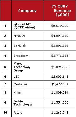 For the record, here are the top 10 global fabless companies of the world, as reported by the Global Semiconductor Alliance (GSA), formerly, Fabless Semiconductor Association, USA.
According to GSA, the total fabless revenue was $27.3 billion, a 12 percent growth year-on-year during 1H 2008. I believe, quite a few, or nearly all of the companies within the GSA top 10 list, have some sort of a presence in India!
Let’s also re-visit the numbers provided by ISA-Frost & Sullivan in its study on the Indian semiconductor industry. The India semiconductor TAM (total available market) revenues will likely grow by 2.5 times, and the TM (total market) will likely double revenues in 2009. Is this not good enough?
Bear in mind that India also plays an active role in the verification and software domains, and it is increasingly covering the entire design chain. The fabs. vs. fabless debate has been going on since 2004-05. Back then, too, many industry observers were backing the fabless route. Now, this discussion is perhaps, a non-issue, with the fabless segment easily the star performer.
India has long had the expertise in chip/board design, embedded software and system engineering. Also, the product and service differentiation is being increasingly driven through software, where India already enjoys a lead over other the APAC countries.
India distinctly has a tremendous opportunity to lead the global market in both semiconductors and electronic products, with or without fabs, or even being fabless!
Synopsys' Dr Chi-Foon Chan on India, low power design and solar
There have been reports about the troubles within the EDA industry in recent times, especially those related with quarter sales. Interestingly, Synopsys has been the one sailing along fine! If that’s not enough, it made its intention known of playing a role on the solar/PV segment, an area where lot of investments have been happening!
 Given this scenario, I was fortuitous enough, rather, extremely lucky to be able to get into a conversation with Dr. Chi-Foon Chan, President and Chief Operating Officer, Synopsys Inc., during his recent visit to India.
On the state of the global semiconductor industry, he said, it was somewhere now in the low 10s [well below 10 percent]. The EDA industry is currently tracking below that level. However, Synopsys has been growing at around 10 percent. He said, “The technology challenges today are very high.”
Synopsys has a substantial number of R&D population based out of India. Giving his assessment of the Indian semiconductor industry, Dr. Chan added: “Our main interest in India is largely talent and the academia. India can very well get more into the product development side. Even the outsourcing of designs have increased. Our capabilities, of the Indian team, have also increased.”
As with any good semiconductor ecosystem, the Indian industry also needs a proactive industry association, a role played to near perfection by the ISA (India Semiconductor Association). Acknowledging the ISA’s role, Dr. Chan said, “The ISA has also formed a very cohesive team.”
There is little doubt about India’s growing importance in technology strengths and managerial leadership. Dr. Chan added: “We are more on the high-end side and also track what others design. In India, the profiles of designs are definitely high-end in nature. This is largely due to the presence of a large number of MNCs. A very high percentage of designs are in the 45nm and 65nm process technology nodes.”
There is another significant indicator of India’s growing importance, and that is the huge rise in the attendance of the SNUG. In 2000, this event attracted 180 people. However, in 2008, the SNUG attracted over 2,000 people.
Moving India to next level
Given the very high level of commitment on Synopsys’ part toward India, there was a need to find out from Dr. Chan what exactly India needs to do to move to the next level in the value chain in the semiconductor ecosystem.
He advised: “India can do two to three things. One, for the system to grow, you need the government, academia and industry to grow together. India has all of the ingredients required to drive products.”
Comparing India with China, he highlighted the fact that while in China, the local consumption was higher than local supply, that was not the case with India!
“Therefore, looking at merely the local market is not the only thing. Products developed here can also be targeted at the Middle East and Southeast Asia.” He was quite forthright in his analysis, adding: “Industries start when you find markets. The skill sets are already present here. There can well be multiple startups.”
Dr. Chan also touched upon the fab vs. fabless issue, noting that there could well be more of fabless companies in India. “Building a fab requires lot of capital. Also, consolidation will continue to happen.”
What role does Dr. Chan see Synopsys playing in the Indian context? He said: “Synopsys will continue to be a catalyst for the industry. A healthy design industry in India continues to help us. We also work well with the Indian universities. Having more people from the universities will always help. We also invest a lot in application support. The application team also trains others. I now look forward to seeing more fabless companies here and India to become even more global.”
On low power design
India is also a centre of expertise in low power design, given that low power is hugely important in today’s electronics ecosystem. Dr. Chan commented that low power has always been the number one design issue. It cannot be taken care of at one single stage.
He added: “A slightly new concept that has emerged is low-power verification. There are so many schemes for attacking low power, such as multiple voltage islands. We (Synopsys) are spending a lot of effort in low power.
“As a designer, you require detailed analysis. Low-power verification is now coming up. Another area is testing. As an example, if so much power is required, how do you have the power cut from the tool you are using to test? From a Synopsys point of view, we are involved in several points, such as front-end synthesis, testing, sign-off, verification, etc. We are trying to put in a whole lot of methodologies.”
Synopsys in solar
EDA may be able to help by lowering power requirements and leakage on better products. Especially, the Synopsys’ TCAD product can be used to create more efficient and effective solar cells. Now, this is not a new development anymore. Synopsys, along with Magma, have already made known their intentions about setting foot in the solar/PV space.
On the TCAD, Dr. Chan said: “We have a very strong position in the TCAD, commercially. Now, it is one of our most critical elements in high-performance. Our TCAD is among the strongest in the EDA industry.
“In solar, it does not have to be a complicated place-and-route, etc. From an entire solar industry point of view, we have now used some effort from TCAD into this space. Heat transfer issues, etc., are more in the EDA space.”
I will continue my conversation with Synopsys on its solar initiative sometime later. Keep watching this space, folks
On possible Samsung-SanDisk deal; AMD's fab-lite path
Last week, the global semiconductor industry has been hearing and reading about two big speculative stories:
a) A possible acquisition of SanDisk by Samsung, and
b) A possible chance of AMD taking the fab-lite route.
First on Samsung’s buyout (possible) of SanDisk! There have been rumors of a possibility of Samsung acquiring SanDisk. While it is still a possibility, it also leads to several interesting questions!
Should this deal happen, what will be the possible implications for the memory market? Will this also lead to a possible easing off on the pricing pressures on the memory supply chain? And well, what happens to the Toshiba-SanDisk alliance?
A couple of weeks back, iSuppli, had highlighted how Micron had managed to buck the weak NAND market conditions, and was closing the gap with Hynix in Q2, and that NAND recovery was likely only by H2-2009.
I managed to catch up again Nam Hyung Kim, Director & Chief Analyst, iSuppli Corp., and quizzed him on the possible acquisition of SanDisk by Samsung.
A caution: Remember, all of this is merely based on speculation!
On the possibility of Samsung’s takeover of SanDisk, he says: “Samsung at least said that they consider it. Thus, it is a possible deal. But who knows!”
Kim is more forthright on the implications for the memory market, should this deal happen, and I tend to agree with him.
Consolidation inevitable; no impact on prices
The chief analyst quips: “The NAND flash market is still premature and there are too many players in flash cards, USB Flash drives, SSD, etc. The industry consolidation should be inevitable in future.”
So, will this possible buyout at least ease some pricing pressures on memory supply chain? “I don’t expect this deal to impact the prices. Prices will depend on suppliers’ capacity plans. In the memory industry, the consolidation has never impacted the prices in a long run. (maybe, just a short-term impact). As you know, Micron acquired Lexar a few years ago, but no impact,” he adds.
Is there any possibility of SanDisk delaying its production ramps and investments at two of its fabs? And, what will happen should it do so?
Nam says: “SanDisk has already said that they would delay its investment and capacity plan given difficult market condition. This is a positive sign to the market as we expect slower supply growth than expected in future. However, in a long run, consolidation won’t impact the market up and down.”
Negative impact likely for Toshiba?
Lastly, what happens to the SanDisk-Toshiba alliance, should the Samsung buyout of SanDisk does happen?
Nam adds: “It is negative to Toshiba. The company [Toshiba] not only loses its technology partner, but also loses its investment partner. It should be burden for Toshiba to keep investing themselves to grow its business.”
Well, in SEMI’s Fab Forecast Report, there is mention of how Toshiba and SanDisk are among the big spenders in fabs, in Japan. Considering that Japanese semiconductor manufacturers are more cautious, it would be interesting to see how this deal, should it happen, affects the Toshiba-SanDisk alliance.
Now, AMD goes fab-lite?
While on fabs, this brings me to the other big story of last week — of AMD going the fab-lite route, possibly!
Magma’s Rajeev Madhavan had commented some time back that fab-lite is actually good for EDA. It means more design productivity. Leading firms such as TI, NVIDIA, Broadcom, etc., are Magma’s customers.
Late last year, Anil Gupta, MD, India Operations, ARM, had also commented on some other firms going fab-lite! Gupta pointed out Infineon, NXP, etc., had announced Fab-Lite strategies. Even Texas Instruments was moving to a Fab-Lite strategy. “IDMs are going to be the fabless units of today and tomorrow,” he added.
So much for those who’ve taken the fab-lite route, and industry endorsements.
On the fab-lite subject, iSuppli’s Kim will not speculate whether AMD would actually break up into into two entities: design and manufacturing, and also prefers to wait and watch.
How does fab-lite actually benefit? He comments: “Fab-lite has not been working well in the memory industry, which requires very tight control. It works, IF two companies (an IDM and a foundry) work very closely. For example, the industry leader, Samsung, produces all of the memory alone without any foundry relationship.”
Watch this space, folks!
10-point program for Karnataka semicon policy
A very interesting question was recently thrown at me: what sort of semiconductor policy should Karnataka adopt as a state! I shall attempt to highlight some of the activities the Karnataka government can look at implementing in the semicon/EMS space.
Let us first go back to last September, when the Indian government issued fab guidelines. Besides wafer IC and solar/PV fabs, the Indian government is seeking investments in ecosystem units for LCDs, OLEDs, PDPs, photovoltaics, solar cells, storage devices, advanced micro and nanotech products, etc.
The ‘ecosystem units’ have been clearly defined as units, other than a fab unit, for manufacture of semiconductors, displays, including LCDs, OLEDs, PDPs, any other emerging displays; storage devices; solar cells; photovoltaics; other advanced micro and nanotechnology products; and assembly and test of all the above products.
For starters, the Karnataka state needs to have a long-term semiconductor policy in place, running 20-25 years or so. This cannot be a short-term plan! It would be prudent to have the top Indian leaders from Indian firms and MNCs, e.g., Ittiam, MindTree, Synopsys, Cadence, TI, Analog Devices, as well as the Indian Institute of Science (IISc.) and some other leading technology institutes, be the part of a core state semiconductor policy team to oversee the implementations. Future state governments would only need to update the status and keep it rolling forward.
Incentives need to be built in as well, including more tax holidays, etc. Whether it needs to be 25-30 percent or higher, is to be debated. Next, the focus of a semicon policy should be aimed at solving some particular local problem, which can go on to solve a much bigger national problem.
All of this should be done with, keeping in view to improving the infrastructure in the state, such as roads, water, electricity, etc. Foreign investors would shy away if infrastructure issues were not tackled first.
In this context, the Karnataka government should first look at having some solar/PV fabs in the state, as well as those in the nanotech space. Next, it would be prudent to pursue a policy of attracting companies in the verification and testing domains. Rather, have companies in the ATMP space, a pointer, which has been coming up in most of the discussions.
As an example, last year, an Israeli company — Nova Measuring Instruments — was keen on entering India. Nova develops, produces, and markets advanced monitoring, measurement and process control systems for the semiconductor manufacturing industry. It should be pursued to start assembly and testing of products in the state.
Wafer IC fabs are going to be a tough act to follow. Unless a company can get the requisite funding for a 300mm fab, it is not advisable to follow that path. However, there is room for developing 200mm fabs, or even 150mm and 180mm fabs. These can be used to develop indigenous and simple applications. If such fabs are developed, those companies offering fab-related services can be attracted as well.
The Indian semicon policy statement speaks about having ecosystem units. It would be advisable to attract smaller companies and look at setting up manufacturing units. As an example, Synopsys’s Subhash Bal had once pointed out how RFID can be used in a host of applications. That’s not all. Why not pursue companies in the OLEDs/LEDs and PDPs spaces as well, besides those manufacturing LCDs, even if smaller-sized.
Finally, consider attracting and promoting companies in the fabless space, as it looks to be the way ahead for the semiconductor industry.
Here is a 10-point program for the Karnataka government to consider as a likely semiconductor policy.
1. A long-term semiconductor policy running 20-25 years or so.
2. Core team of top Indian leaders from Indian firms and MNCs, as well as technology institutes in Karnataka to oversee policy implementation.
3. Incentives such as government support, including stake in investments, and tax holidays.
4. Strong infrastructure availability and management.
5. Focus on having solar/PV fabs in the state.
6. Consider having 150/180/200mm fabs that tackle local problems via indigenous applications.
7. Develop companies in the assembly testing, verification and packaging (ATMP) space.
8. Attract companies in fields such as RFID, to address local problems and develop local applications.
9. Pursue companies in the PDP, OLED/LED space to set up manufacturing units.
10. Promote and set up more fabless units.
There should be some steps to create specific zones for setting up such units — for fabs, fabless, ATMP, manufacturing, etc., all spread equally across the state.
On a personal note, I would be keen and willing to work with the Indian/Karnataka government, or the concerned parties, in formulating such a policy, should I am invited. Nothing would give me greater pleasure than seeing India, and Karnataka, shining in the semiconductor space.
Top 10 global semicon predictions — where are we today
 It is always interesting to write semicon blogs! Lots of people come up to me with their own comments, insights, requests, etc. One such request came from a friend in Taiwan, who’s involved with the semiconductor industry.
I was asked forthrightly what I thought of the top 10 global predictions, which I had blogged/written about some time back late last year.
Top 10 semicon predictions
For those who came in late, here are the 10 global predictions on semiconductors made at that time (late December 2007.
1. Semiconductor firms may have to face a recession year in an election year.
2. DRAM market looks weak in 2008.
3. NAND market will remain hot.
4. Power will remain a major issue.
5. EDA has to catch up.
6. Need to solve embedded (software crisis?) dilemma.
7. Consolidation in the fab space.
8. Capital equipment guys will continue to move to other market.
9. Spend on capital equipment to drop.
10. Mini fabs in developing countries.
Well, lot of water has flowed since those predictions were made. Let’s see how things stand, as of now. The updated predictions would look something like these:
1. There have been signs of recession, but the industry has faced it well, so far. In fact, Future Horizons feels that if there is going to be a global economic recession, the chip industry (but not all companies) is in the best shape possible to weather the ensuing storm.
2. Memory market is changing slightly as well, though people are very cautious. According to Converge, memory market prices appear to be stabilizing. iSuppli has predicted a poor year for DRAM though!
3. NAND Flash could show some recovery later this year. Yes, Q1-08 QoQ sales seems to have slipped, but the market remains hopeful of a recovery. Even iSuppli warned of NAND Flash slowdown in 2008, while Apple slashed its NAND order forecast significantly for 2008! Keep those fingers crossed!!
4. Power remains a big issue, and will continue to be so. This will remain as we move up newer technology process nodes.
5. EDA is seemingly catching up with 45nm designs. Magma, Synopsys, and the other leading EDA vendors are said to be playing big roles in 45nm designs.
6. Fabless companies are gaining in strength. No doubt about it! The 2007 semicon rankings show that. Also, Qualcomm is now the leader in the top wireless semicon suppliers, displacing Texas Instruments.
7. There have been consilidations (or long term alliances) in: a) fab space b) DRAM space. In the fab space, Intel, Samsung and TSMC have combined to go with 450mm wafer fab line by 2012. And in the DRAM space, there have been new camps, such as Elpida-Qimonda, and Nanya-Micron partnering to take on Samsung. With the global semiconductor market seeing steady decline in growth rate, which would continue, look forward to more consolidations.
8. Investments in photovoltaics (PV) have eased the pressure on capital equipment makers and spend somewhat. In fact, 2007 will be remembered as the year when the PV industry emerged as a key opportunity for subsystems suppliers and provided a timely boost in sales for those companies actively addressing this market. Perhaps, here lies an opportunity for India.
9. Mini fabs — these are yet to happen; so far talks only. In India, a single silicon wafer fab has yet to start functioning, even though it has been quite a while since the semicon policy was announced. Conversely, some feel that India should focus on design, rather than go after something as mature as having wafer fabs. However, several solar fabs — from Moser Baer, Videocon, Reliance, etc., are quite likely.
10. Moving to 45nm from 32nm is posing more design challenges than thought. This is largely due to the use of new materials. Well, 45nm will herald a totally different structure — metal gate/high-k/thin FET/deep trench design, etc. It will herald a new way of system design as well.
Now, I am not a semicon expert by any long distance, and welcome comments, suggestions, improvements from you all.
