Archive
My blog's been nominated by Electronics Weekly!
It was indeed a pleasant surprise to receive an email from Electronics Weekly, yesterday evening, informing me that my blog was recently shortlisted/nominated in the 2008 ElectronicsWeekly.com Blog Awards by a reader of ElectronicsWeekly.com!
All of the nominated blogs have apparently been considered by the panel of judges at ElectronicsWeekly.com. The email said, “I am delighted to inform you that you have made the shortlist in the Best Electronics Hardware Blog category.”
The list can be seen on Electronics Weekly’s (www.electronicsweekly.com) website!
Wow! I must add that here that there are such great blogs and bloggers in that list that I went dizzy for a few minutes!
I never expected my blog to reach this kind of appeal or level! Nor do I think I have that kind of traffic, as this blog has more to do with serious stuff, rather than talk about gadgets, etc. In fact, somebody once told me last year that no one would bother about a blog on semicon and electronics, nor would I get any traffic!
Well, all of this has never bothered me. I’m here to blog about what I feel is close to my heart! If folks happen to stop by, I am extremely grateful to all of them!
Irrespective of whether I win this award, it is just the right time to thank all of you, dear readers of my blog! Thanks to all of you for choosing to stop by my blog occasionally! I sincerely hope you find the content interesting and appealing enough.
There’s lots happening in the semiconductor, electronics and telecom industries, and hope that I am able to add my views on all of those in the coming months.
Thanks again, my dear readers. Please keep those suggestions coming. I will try to live up to your expectations. Have a great Halloween, everyone!
Semicon half year over, what next now?
Wow! A majority of my predictions made on this blog for the global semiconductor industry have so far turned out correct — in December 2007 and again in May 2008.
Recently, I’d done a check on where are we today, in May, and earlier, via a Webcast from Semiconductor International, I had mentioned about the semiconductors market situation. Around that time, I had attempted my hand at predicting the top 10 global semiconductor trends for 2008.
There have been several folks, who’ve contacted me via this blog. Each one of them has his and her opinion about the semiconductor industry, and now want me to take this up a little bit more ahead. Let’s see what more I can do!
While all of these makes me feel proud of having been spot on with my assessment of the global (and Indian) semiconductor industry, it should also serve as a warning for the global (and Indian) semiconductor industry — that it really needs to pull up its socks! It is not going to be an easy ride ahead!
For starters, you simply cannot wish away the rising oil prices. The oil prices impact will be immense, and DRAM and flash are still wobbling. Besides, the ASPs are a wobbly lot and will continue to remain so. Interestingly, several forecasts from various quarters have been revised or re-assessed. Didn’t you all see it coming?
I’d also like to touch upon the Indian semiconductor industry. In all likelihood, the wafer fab story has all but disappeared. Very few comments are now being made about the wafer fabs, although, how this topic was played up, rather, hyped up about a year ago is quite well documented. In fact, I’d also written about whether the timing was right for having fabs in India!
No, it is not a failure on part of the Indian industry or the India Semiconductor Association. Perhaps, we started on the fab path a bit too late! Let’s all accept that!! Having said that, if a wafer fab or two do start functioning in India later in 2009 or beyond, that would be simply great!
Yes, several solar fabs are coming up and investments in solar/PV are rising, as also in India, but that was along expected lines.
I’d mentioned earlier that investments in photovoltaics (PV) had eased the pressure on capital equipment makers and spend somewhat. In fact, 2007 is now well remembered as the year when the PV industry emerged as a key opportunity for the subsystems suppliers and provided a timely boost in sales for those actively addressing this market. Perhaps, here lies an opportunity for India! I’m repeating this to the extent of sounding boring.
Further, even though it has been quite a while since the Indian semicon policy was announced, some feel that India should continue to focus on design services and embedded — its well known strengths, rather than go after something as mature as wafer fabs. Also, why do we have to ‘force ourselves to think’ that we are good at product development? We are not! Yes, it can change, but that would need great effort on part of all industry stakeholders.
So, what next? For now, I will not try and predict again what’s the way ahead for the semiconductor industry, as I’ve recently done a self check on where the global semiconductor industry stands today. That assessment will be left for another day!
Top semicon articles of 2008
A very kind reader left a comment yesterday that he (or she?) spent three hours on my blog! I am simply overwhelmed and humbled!!
It has really been a pleasure writing and maintaining a semicon blog! Plenty such are around carrying very valuable information, and I salute those bloggers.
It is really tough to contend with all the other technology-related information, but then, semicon has its own charm, and its own set of dedicated readers — who DO go on to become extremely loyal.
I am even more touched by another request by a friend to list all the top articles I’ve written this year. Wow!!
It is very difficult for me to say, which ones are the best! However, I am listing the articles here. They all link back to CIOL. Of course, I’ve blogged here first, so, those who are familiar with my blog pieces, will identify them immediately.
Here goes then — starting from the latest back down to very late last year — in terms of relevance. Enjoy!
Semi trends 2008: Fab spend lower, ASPs stabilizing
The call on global fab spend was for a 10 percent reduction, and this is now getting to be closer to 20 percent.
UK, India aim for semicon collaboration
ISA-UKTI study examines collaboration scope between India and UK in design, applications and devices.
Dubai an emerging silicon frontier
The government of Dubai has set up the Dubai Silicon Oasis Authority (DSOA) as the engine for propelling Dubai into the knowledge economy.
Be parallel, or perish!
Parallelism offers new doors, and creativity is required to open these new doors, says Intel.
Altera first @ 40nm FPGAs
The company has announced two product lines — the Stratix IV FPGAs and the HardCopy IV ASICs.
Semicon likely to grow 12pc in 2008
If there will be an economic recession, the chip industry (but not all firms) is in the best shape possible to weather the ensuing storm.
India’s growing might in global semicon
India is fast becoming the world’s destination, and increasingly the source too, for semiconductors.
Fascinating developments in 22nm!
These augur well for the global semiconductor industry, even though the field could get much narrower.
Indian design services to touch $10.96bn by 2010
Total design services market in India is said to have grown at 21 percent year on year.
NXP India achieves RF CMOS in single chip
The entire analog and RF work done has been in Bangalore by NXP’s single-chip design team.
LabVIEW 8.5 delivers power of multicore processors
With LabVIEW, designers and engineers can assign different tasks on different cores — which are independent.
Multi-nationalization of product development process
Indian designers lead in transaction level design, and can play big role in EDA.
Can we expect exciting times in 2008? Some trends
Blurring lines between PMPs and PNDs, semicon rush or hush; Netscape’s end — all are in store!
Semicon outlook 2008: Global market likely to grow 6-11 percent in 2008
Some predictions are for 2008 to be flat year or a year of negative growth; EDA to grow 7.8pc!
That’s about it! If there’s anything I’ve missed out, kindly let me know. Thanks for all your continuing support, dear readers. It is very humbling and touching.
ASPs stabilizing, fab spend lower than expected
Future Horizons recently released the May WSTS results on the global semiconductor industry, which indicate that the chip market is slowly starting to buzz again. With the ‘hum back among the chips’, it was important for me to quiz Malcolm Penn, chairman and CEO, Future Horizons, in the UK, to find out why this was happening!
Now then, why is the chip market exactly humming? What has actually happened? Well, nothing specific! It is merely an overall step-by-step general improvement in everything, helped along by the normal seasonal improvement in business in the second half of the year!
So many forecasters and firms have their own forecasts. What happens now if some of these forecasts are cut or revised? Will that affect the market overall market? The answer is simple — a forecast is simply just that — a forecast — not fact!
Penn says, “The market will judge whether the other forecasters’ analyses of the market were right, as it wll indeed judge whether we are right too!”
Earlier, I had written about Future Horizons forecasting 12 percent growth in 2008 for the global semiconductor industry. Keep an eye on that one!
Further, have the ASPs stabilized, as those are indeed a dodgy lot? Penn feels, “We believe yes, although, there will still be the normal month-on-month variations and wobbles.”
Now, where does all of this leave the DRAM and NAND markets? According to the forecast, prices have already stopped falling as fast as they were this time last year.
However, they do fall and will fall; this is what they do! The question is: by how much? In other words, is the current fall above or below the long-term trend line? This will be analyzed in the long run as well.
Finally, what’s happening with the semicon equipment capex? Again, it is continuing to fall! “Right now we are in the middle of an underinvestment period, which means a capacity shortfall in 12 month’s time,” notes Penn.
No ‘fab’ times for fab spends
Is the fab spend going to see any change then? Well, unfortunately, no luck there! At least, not yet. Penn adds that fab spend is lower than expected at the beginning of the year.
He says: “The call then was for a 10 percent reduction, and this is now getting to be closer to 20 percent. In fact, Mike Splinter of Applied Materials is quoted as saying that he thinks that fab spend will end up 30 percent down.”
It is good to see that the global semiconductor industry is starting to hum a little bit more than what it was doing last month. Sincerely hope that the rest of the year pans out well!
Chip market is beginning to hum again!
Future Horizons has released the May WSTS results today on the global semiconductor industry, which indicate that the chip market is slowly starting to buzz again.
 Malcolm Penn, chairman and CEO, Future Horizons, points out that as shown in May’s WSTS results, March’s sale figures romped home with a vengeance – reversing February’s lacklustre performance – with IC sales up 10.8 percent on February and 8.2 percent on the same time last year.
More importantly, the ASPs were up 13.3 percent on February and 2.1 percent on March 2007.
While the increase on February 2008 is merely part of the normal month 3 versus month 2 quarterly patterns, the increase over the same period last year is much more statistically -– and structurally -– significant.
“Finally, the chip market is starting to hum. Now is NOT the time to cut back on the 2008 forecast,” he adds.
Now then, why is the chip market exactly humming? What’s actually happened? Well, nothing specific! It is merely an overall step-by-step general improvement in everything, helped along by the normal seasonal improvement in business in the second half of the year.
So many forecasters and firms have their own forecasts. What happens now if some of these forecasts are cut or revised? Will that affect the market overall market? The answer is simple — a forecast is simply just that — a forecast — not fact! Penn says, “The market will judge whether the other forecasters’ analyses of the market were right, as it wll indeed judge whether we are right too!”
Earlier, I had blogged about Future Horizons forecasting 12 percent growth in 2008 for the global semiconductor industry. Keep an eye on that one!
Further, have the ASPs stabilized, as those are indeed a dodgy lot? Penn feels, “We believe yes, although, there will still be the normal month-on-month variations and wobbles.”
I shall continue this story in my next blog… so keep reading folks! My very warm regards and thanks to all of you who do stop by to read and comment.
Indian design services to cross $7.37bn in 2008
The Indian semiconductor and embedded design services market has grown consistently over the last five years and market is likely to cross the US$ 7.37 billion in 2008.
This was the key finding of the “India semiconductor and embedded design service industry (2007-2010): Market, technology and ecosystem analysis”, a study jointly released today in Bangalore by the India Semiconductor Association (ISA), and IDC (India) Ltd.
Some key findings of this comprehensive report include:
* The total design market in India for 2007 was estimated at US $6 billion. Eighty-one percent of the revenues were in the area of embedded software, followed by VLSI design (13 percent) and hardware/board design (6 percent).
* The total workforce employed in the design services industry in India was estimated at 130,000 in 2007.Of this the bulk of the jobs were in embedded software 82 percent followed by VLSI design (11 percent) and hardware/board (7 percent).
* The industry was estimated to grow at a CAGR of around 21.7 percent between 2007-2010.
* The geographical focus of the industry indicates that US has a share of 70 percent; Europe at 30 percent; and the emerging economy is that of Japan.
Key factors that determine the growth of the design sector in India are: the growing expertise and capabilities in complex end-to-end design; strong IP development and talent. The Indian domestic market is one of the fastest growing in Asia as well as globally.
Commenting on the Indian design market, Poornima Shenoy, president, ISA, said: “The Indian semiconductor design industry, with over 200 companies, is on a strong growth trajectory. Our growth is nearly 22 percent which is three times the global growth rate of around 7 percent. We are looking eastward for business and collaboration heralding a new era in the future of the sector.”
Announcing the findings of the ISA-IDC report, Kapil Dev Singh, added: “The Indian semiconductor and embedded design services market has grown consistently over last the five years and market is expected to cross the US$ 7.37 billion in 2008. The domestic semiconductor and embedded design services industry is all set to enter a new phase -– Ver 2.0, following on from where Ver 1.0 left off. To achieve this next phase of growth, the industry needs to focus on the availability of quality manpower, higher productivity and more value creation.”
Semiconductor outlook 2008: EDA to grow 7.8pc; semicon 6-11pc
Forecasters at the panel discussion the 2008 Semiconductor Industry Forecast webcast presented by Semiconductor International were guarded in their predictions — which were a mixed bag — with the majority predicting semiconductor growth in the range of 6-11 percent during 2008.
However, some other panelists predicted 2008 to be flat year or a year of negative growth. There are fears of a possible recession in 2008, along with concerns surrounding consumer spend that could be hit by higher oil prices and the US mortgage crisis. Hence, the need for forecasters to be watchful with their predictions.
EDA playing catch-up; to grow 7.8pc
The EDA industry is said to be lagging behind the semiconductor industry at the moment, and is in the catch-up mode, according to Gary Smith, President, Gary Smith EDA, while commenting on the forecast for the EDA industry.
On the outlook for the EDA market, Smith said the EDA industry is in a lttile unusual position. He said: “The market’s been flat for the past four years. Tools for 65nm, 45nm silicon dsign have also been delayed.” The R&D was not put in because of the recession. “Right now, we are in a position of lag in the market,” he added.
EDA tools cover two process generations. The industry is just starting to introduce 65nm and 45nm tools. That generation is being called the DFM generation tool. Smith said: “It is even more important to the semiconductor industry as we run into manufacturing problems that they are relying on design tools to solve, rather than on semiconductor equipment.” That’s a major shift in the market!
According to him, the industry is now now into a pretty good growth area. “We were 11 percent last year, 10.2 percent to come in this year. We will be a bit down next year at 7.8 percent,” he forecast. This has been attributed mainly to the EDA industry’s lag in the market. “Some are moving to 32nm. And certainly, a lot of work is being done in 45nm,” he added.
Smith noted: “The EDA industry is in the catch-up mode. We will lag them. We’re expecting the downturn to really hit us in 2009. However, we’re not an industry that goes negative often. No matter what you guys do, you still have to design something. So, when you go into recession, typically, the way you get out of recession is you generally design yr way out!”
DFM, ESL, parallel computing EDA growth drivers
He said that DFM, parallel computing and ESL were the growth drivers. Among the drivers is the DFM issue, which is increasingly getting more complex. There is said to be a move to restrict the design rules that is in place now for 45nm. “We’re going to see major changes in 32nm; that’ll have impact on tools,” he added.
The other issue is parallel computing that has become a major task for the EDA industry. “With signal threading, we can no longer handle designs over 100 million gates. Of course, at 45nm, you can do a 100mn gates. That rewriting process is another issue that is also slowing out down. That’s a full three-year re-write,” Smith said.
Further, EDA is also starting to move up into the ESL. The ESL is going to shift the EDA market more into the systems market, and serve less on its dependency on the semiconductor world.
As for the inhibitors, an issue hitting the EDA industry right now is that, in 2007, the cost of designing or developing the embededded software for an SoC actually passed the cost of desgining the SoC itself. “So, we’re in the middle of a software crisis that’s going to hit the entire electronics ind in the next five or six years,” he added.
Next, the industry has been also going to muticore, multiprocessor architecture. That demands a completely new programming model. According to Smith, what was unthinkable six months ago, is now a major topic of discussion — that is abandoning C as a programming language! That’s going to be a major shift in the industry.
Tariff concerns in Europe
Earlier, in a discussion regarding concerns about tariffs in Europe, and how will it impact the industry, Anne Craib, Director of Market Research, International Affairs and Finance, Semiconductor Industry Association (SIA), said: “We are working on a number of policy initiatives that we see as potential challenges in consumer sector.” In Europe, there is an effort to re-classify goods that have business and consumer funtionalities, as consumer products not covered by tariff-free agreement.
As we see continued convergence, for example, the cell phone will be covered, so, there are questions as to whethe a cell phone has a cam or an MP3 player, and will that be considered as a consumer device or a business device. The result could be the imposition of fairly steep tariffs in the mid to high teens. “When you start to increasing your pricing to that level, it could potentially affect consumer demand. We havent seen that happen yet, but it’s an issue that we are quite concerned,” she added.
SIA is also concerned about some efforts in other parts of the world to put in place proprietary standards that could drive up the cost for manufacturers for accessing those markets — by requiring to make devices that are specific to certain markets — that wouldnt be interoperable. Most of them could affect the downstream products, but not semicon specifically. However, there are areas that the industry also needs to be aware of.
Stay tuned for full report later!
Importance of power awareness in chip designing
Power awareness is said to be crucial for portable applications. It determines the battery lifetime, and there’s an increased amount of computation involved as well.
The other factor is that power awareness is extremely crucial for high-performance applications. This determines cooling and energy costs as well. Many chip designs today are power limited and still require maximum performance.
Battery storage has been a limiting factor as well. The reasons are manifold. For one, battery energy doubles in a decade! It does not follow Moore’s law! Next, there has been little change in the basic battery technology. A battery stores energy using a chemical reaction. Hence, the energy density/size safe handling are limiting factors as well for batteries.
Low power challenges in VLSI domain
There are low power challenges in the VLSI domain. The challenge is four-fold in nature. The devices are leaky. Further, more integration means more W/cm2, while the EDA tools used are not that good in the low-power domain and also doesn’t co-relate sometimes with the silicon. Finally, the variability of the device parameters simply make things worse.
Power dissipation is of two types — static and dynamic. Static power dissipation can be minimized by reducing the operating voltage and using fewer leaking transistors. Dynamic power dissipation can be minimized by reducing the operating voltage, and by less switching capacity, and less switching activity.
Several leakage mitigation techniques are currently in use, such as lower operating voltage, cell sizing, dual Vt, power gating, non-minimum size gate lengths, VTCMOS and stack effect.
According to Jayanta Lahiri, director, PIPD, ARM, the company uses two methods — IEM and PMK.
ARM Artisan power management kit uses power gate components, which can switch between ‘global’ and local rail. It makes use of VDD Header and VSS Footer switches, and high-Vt switch for low off-current leakage. It also uses coarse-grain power gates for multiple cells, which are available in different sizes.
Another ARM Artisan power management kit uses state retention components. The ‘global’ power rails to retention latch. It has power-switched primary master/slave latches, and high-Vt switch for low off-current leakage. It also makes use of the single-pin retention control (RETN), which can save the state on falling-edge of RETN and also restore state on rising-edge of RETN.
Power gated memory facilitates the standby mode, the retention mode and the shutdown mode. In the standby mode (HALT), the CEN disables the memory and leakage only standby current.
In the retention mode (SRPG), power is supplied to the core array to retain state. Power is off for periphery for reduced leakage and the outputs are clamped to zero.
In the shutdown mode (OFF), power is off for the core and periphery for reduced leakage, and the outputs are clamped to zero.
This is possible through both integrated MTCMOS power-gates as well as separated power sources for the core and periphery.
Top 10 semicon firms of 2007 by revenue
According to Gartner, the top 10 semiconductor firms for 2007 by revenue are: Intel, Samsung Electronics, Toshiba, Texas Instruments, STMicroelectronics, Infineon Technologies (including Qimonda), Hynix Semiconductor, Renesas Technology, NXP Semiconductors, and NEC Electronics.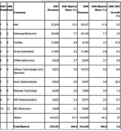
Worldwide semiconductor revenue totaled $270.3 billion in 2007, a 2.9 percent increase from 2006, according to preliminary results from Gartner Inc.
Vendor performances were mixed with two vendors in the top 10 that experienced double-digit growth and two vendors that showed declines in revenue.
“Semiconductor vendors need to watch the performance of their end customers even closer as a major part of the industry becomes increasingly tied to consumer spending patterns,” said Andrew Norwood, research vice president at Gartner. “Loss of market share in an end-user application, such as a mobile phone, by a customer (a mobile phone manufacturer) can have a dramatic effect on a vendor’s business.”
Intel grew revenue more than twice as fast as the semiconductor market average, and it is likely to edge up its market share to 12.2 percent in 2007 from 11.6 percent in 2006.
Intel’s growth came primarily from strong shipments of mobile PCs. Armed with a strong product lineup for enthusiast desktops and servers, Intel regained lost share in those markets from AMD.
While the global market for dynamic random-access memory (DRAM) is expected to decline in 2007 due to a severe drop in prices caused by oversupply, Samsung Electronics is likely to increase its revenue by slightly higher than the overall global semiconductor market growth rate (DRAM is one the firm’s main products).
Samsung’s growth is driven by steady revenue growth in NAND flash memory and strong revenue growth in nonmemory areas such as application processors, media integrated circuits (IC), complementary metal-oxide semiconductor (CMOS) image sensor, smart card ICs and LCD driver ICs.
Toshiba’s revenue increased 27.8 percent in 2007 to $12,504 million, gaining three places in the rankings and moving into third place. The rapid gains mainly came from NAND flash memory.
Toshiba also increased production of CMOS image sensors for mobile phones and application-specific integrated circuits (ASICs)/application-specific standard products (ASSPs) revenue for digital consumer electronics, including LCD TVs, next-generation DVDs (HD DVDs) and video game consoles.
Outlook for Indian semiconductor industry in 2008
S. Janakiraman, president and CEO –- R&D Services, Mindtree Consulting, and chairman, India Semiconductor Association (ISA), is quite bullish on the advantages of India and the opportunities provided in the Indian semiconductor industry. Here are some notes on the outlook for the Indian semiconductor industry in 2008.
Indian semiconductor industry to grow 25-35 percent in 2008
There has been an increasing trend of an increasing brand value for semiconductors within India. MNCs, especially are looking at semiconductor related outsourcing from India. We are also seeing lot of traction, from third-party service providers, like us — Mindtree, Wipro, Sasken, etc., as well as captive centers of MNCs like STMicroelectronics, NXP, etc.
In terms of growth plans, all leading MNCs, like NXP, Freescale, STMicroelectronics, etc., are planning to grow significantly from their India centers. They are strongly building partnerships with Indian designers.
From the design side, India is also seeing an increase in various activities, such as more complex analog designs and more complex digital designs. We are seeing more of physical designs happening, and even taking those designs up to the foundries are increasing as well. “We foresee 25-35 percent likely growth in the Indian semiconductor industry during 2008,” said Janakiraman.
Software is very critical to succeed. Various Indian providers, including Mindtree, are developing software for semiconductor-related products that are being designed by the overseas semiconductor companies.
Fab policy — More of ATMP
The fab policy announced by the government of India is really attractive and mostly on par with other countries. A semiconductor fab requires very high capital-intensive investment. In 2008, we will be probably seeing more of the assembly, testing, marking and assembly (ATMP) happening in India.
The fundamental fabs are still a little far away. Most companies are likely to start off by initially testing waters by making some level of investments in ATMP before moving on to fabs. One cannot also rule out the prospect of some leading Indian company investing in fabs.
Lot of the big MNCs have been moving to Fab-Lite, having already announced Fab-Lite strategies. They are moving to manufacturing to with people like TSMC, Chartered, etc. If manufacturing happens in the fabs, it would not be from any of the integrated device manufacturers (IDMs). It may also happen from Indian companies who are into manufacturing.
Electronics manufacturing has already moved on to the electronics manufacturing services (EMS) vendors. Similarly, chip vendors are also moving on to third-party providers. MNCs like TI, LSI Logic, etc., are moving away from manufacturing and moving that to Charter, TSMC, etc.
Fab companies will also look at India as the fab policy will look attractive to them. “Those questioning India’s need for fabs would feel terribly missing out on the opportunities currently being provided by India, by 2015,” said Janakiraman.
Product companies in India
Over the next one to two years, we are likely to see more product companies emerging from India. Companies like Tejas are already present in India. Down the line, this will percolate into semiconductors. Opportunities are bound to emerge. It means, first, there will be companies manufacturing electronics products, which will later move on to the emergence of semiconductor product companies.
As for Indian companies into manufacturing electronics products, the ISA chairman feels that there would be more of high-complexity, medium volume products. These would probably be manufacturing networking, automotive, navigation products, etc., which are more rich in software, but are medium volume in production.
Impact of semiconductor policy
According to Janakiraman, the interest in India has only increased since the announcement of the semiconductor policy. As per the announcement, the government of India will bear 20 percent of the capital expenditure during the first 10 years for units located inside SEZs and 25 percent for those located outside.
For semiconductor manufacturing (wafer fabs) plants, the policy proposes a minimum investment of US $625 million. The minimum investment for for ancillary plants is US $250 million. The government’s participation in the projects would be limited to 26 percent of the equity portion. The key benefit is the grant of the SEZ status.
The Indian semiconductor policy is applicable for manufacturers of all semiconductors, displays – including LCDs, organic light emitting diodes (OLEDs), plasma display panels (PDPs), and any other emerging displays, storage devices, solar cells; photovoltaics; other advanced micro- and nanotechnology products; assembly and test.
Advantage India
India is now presenting a great opportunity to the world, in fact, offering triple advantages. India has a very rapidly growing domestic market, growing at a CAGR of 30+ percent. India has achieved global recognition for back-end services -– having become a proven case for IP, embedded systems and IC designs.
India is also an attractive destination for manufacturing investments. It further boasts of a highly skilled employee base, and a fast and upcoming modern infrastructure –- SEZs. India also enjoys proximity to the EU and the MEA markets. It also boasts of freight cost, said to be 20 percent cheaper than China, leading to faster delivery and lesser pipeline inventory.
Indian ecosystem maturing
India is aligning itself with the global semiconductor market by creating high value work in VLSI, and board design and embedded software. Companies with domain expertise are driving Indian businesses. India has become the world’s destination for semiconductor design and embedded software, and is increasingly becoming the source as well.
In terms of consumption, the India semiconductor total available market (TAM) revenues are likely to grow by 2.5 times, while the total market (TM) is estimated to double in revenues by 2009. India’s semiconductor market share is likely to be 1.6 percent of the global market by 2009 in comparison to 1.1 percent in 2006.
Regarding the growth drivers for electronics manufacturing in India, telecom and IT & OA (office automation) segments will account for almost two-thirds of the semiconductor TAM by 2009. Telecom’s share has been estimated to grow from 21.2 percent in 2006 to 41.1pc by 2009.
According to ISA estimates, TAM revenues are likely to grow by 2.5 times and TM revenues are likely to double their revenues by 2009 as against 2006. Growth of TAM revenues is 35.8 percent compared with just 26.7 percent for TM revenues, thereby signifying an increasing manufacturing index for different electronics products in India.
The decline in ASP (average selling price) of semiconductors and hence, of electronic products, is largely offset by the higher unit sales of different electronics end use products.
Indian electronics industry — 2010 scenario
India will have a very strong electronics scenario by 2010. The installed base of mobile phones will go up to 500 million. The installed base of PCs will move up to 65 million. The IT enabled services (ITeS) and software exports has been estimated at US $60 billion.
There will likely be about 40 million new Internet connections, with at least 50 percent of those being broadband connections. The nationwide TV broadcast is likely to become digital by 2015, beginning 2010. In that scenario, there would be significant opportunity for set-top boxes (STBs) consumption and manufacturing. There will also
be an estimated over US $10 billion investment in e-governance initiatives and the national ID card.
