Archive
India's teaching community contemplates SoC design
The VLSI Society of India recently organized a two-day faculty development workshop on SoC design, — Train-the-Trainer program — on Oct. 30-31, 2010, at the Texas Instruments India office, in co-operation with PragaTI (TI India Technical University) and Visweswaraya Technological University (VTU).

Dr. C.P. Ravikumar, TI, addressing the teachers at the workshop on SoC design.
I am highly obliged and very grateful to the VLSI Society of India and Dr. C.P. Ravikumar, technical director, University Relations, Texas Instruments India, for extending an invitation. Here is a report on the workshop, which the VSI Secretariat and Dr. Ravikumar have been most kind to share.
System-on-chip (SoC) refers to the technological revolution, which allows semiconductor manufacturers to integrate electronic systems on the same chip. System-on-board, which has been the conventional implementation of electronic systems, uses semiconductor chips soldered onto printed circuit boards (PCBs) to realize system functionality.
Systems typically include sensors, analog frontend, digital processors, memories and peripherals. Thanks to the advances in VLSI technology, these sub-systems can be integrated on the same chip, reducing the footprint, cutting down the cost, improving the performance and power efficiency.
While the industry has adopted SoC design for many years, the academic community around the world (India not being an exception) has not caught up with the state-of-the-art. Electrical/electronics engineering departments continue to teach a course on VLSI design, where the level of design abstraction is device-level, transistor-level, or gate-level.
Register-transfer-level (RTL) design using hardware description languages is taught in some Masters’ programs, but colleges often do not have the lab infrastructure to carry out large design projects; very few Indian universities have tie-ups with foundry services to get samples. A semester is too short a time to complete a large project.
The complexity of modern-day design flow is not easy to impart in a single undergraduate course. Masters’ programs are particularly relevant in VLSI, but the M.Tech programs in the country languish due to several reasons.
Ground realities
“M.Tech programs do not attract top students who are highly motivated,” said a professor who attended the two-day faculty development program organized by VLSI Society of India. “Almost all undergraduate programs today have a course on VLSI technology and design. But since we get students from different backgrounds, they do not have the pre-requisites. So, a course on VLSI design at M.Tech level will have a significant overlap with an undergraduate course on VLSI design.”
“Faculty members need training,” said another teacher. “When a new course is introduced, significant time is needed for preparation. Prescribed textbooks for a new course are often not available. Internet search for course materials often returns too much material and it is hard to decide what to use. Colleges that have autonomy can decide their own curriculum, but in a university setup, the faculty face a major challenge. We are evaluated on how well our students fare in the exams. Yet, our students have to face an exam made by a central committee.”
“Having a common exam poses many problems in setting up a relevant question paper. The format of the question paper is fixed. The students get a choice of answering five questions from a set of eight. Due to the common nature of the question paper, the questions tend to demand descriptive answers.”
Faculty development workshop on SoC design
About 30 faculty members interested in system-on-chip design took part in the faculty development workshop. The attendees came from about 25 different colleges from VTU, VIT University, and Anna University. The workshop was conducted in co-operation with the Viswesaraya Technological University (VTU) and sponsored by Texas Instruments, India.
The premise for the workshop was that a course on SoC design is required at the Masters’ level, since industrial practice has clearly moved in that direction. The RTL-to-layout flow, which continues to be relevant for IPs that constitute an SoC, aspects of SoC design, which relies on IP integration, are not covered in any course.
The workshop provided a forum for industry-academia interaction. Several professionals from the industry took part in the workshop and answered questions from the faculty members. Read more…
Indian semiconductor market to reach $7.59bn by 2010!
 Folks, here’s the full report on the India Semiconductor Association – Frost & Sullivan study on the Indian semiconductor industry. I’ve already provided my views on the Indian semiconductor industry report in an earlier post, for those who would like to know more.
First, the findings:
• The Total Semiconductor Market (TM) revenues poised to grow from $5.9 billion in 2008 to $7.59 billion in 2010. The market is estimated to grow at a CAGR of 13.4 percent.
• The corresponding period is likely to witness a CAGR of 13.1 percent in the Total Semiconductor Available Market (TAM). TAM revenues is anticipated to climb to $3.24 billion in 2010 from $2.53 in 2008.
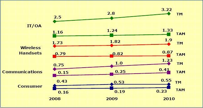 The following chart details how the Indian semiconductor industry is likely to shape up till 2010. All values are in US $ billion.
According to the study:
• Memory and MPU are the leaders in the TM and TAM revenues, respectively.
• IT/OA, wireless handsets and communications are the top three contributors to the TM revenues.
• IT/OA, wireless handsets and consumer are the mainstay of TAM revenue generation.
• Greater affordability of notebooks, netbooks, government IT initiatives, increased usage of memory cards to drive TM revenues from IT/OA. Ratio of desktops to notebooks reduces to 1:5
• Emphasis on rural mobile telephony and decline in handset pricesto drive demand; economically priced handsets in GSM and CDMA to witness higher growth. Mid priced handset segment, with enhanced features, to benefit.
• Rollout of 3G and WiMAX services to act as harbinger of associated infrastructure equipment TM. SDH 64 to increasingly replace SDH 4 and SDH 16. Increased manufacturing expected to favor TAM revenues.
• Evolving lifestyle expected to assist consumer electronics related semiconductor TM. DTH revolution creates demand for STB like never before. The market is expected to sustain as technology upgrades from MPEG2 to MPEG4.
• Projects like national ID cards, bank cards and kisan cards are likely to favor the semiconductor usage in emerging segment of smart cards.
• Low manufacturing index leads to opportunity loss of $3.37 billion semiconductor market revenues. This loss anticipated to increase to $4.35 billion by 2010.
• Immense, yet untapped, opportunities exist for semiconductors in STBs, LCD TVs, digital cameras and storage Flash memory markets.
• Decline in semiconductor product prices result in lower revenue realization; key semiconductor products impacted are memory, MCU and discrete. Increase in memory usage in a variety of products to offset revenue loss on accountof decline in prices.
• Increased usage of system-on-chip (SoC) leads to decline in the overall revenues. Though the decline is not proportionate to the reduction of components, the impact is significant.
• Higher penetration of notebooks to impact market for desktops and offline UPS
• Current slowdown to impact overall growth and manufacturing investment prospects for 2009; uncertainty in government decision-making adversely affects growth.
Some of the other forecasts of the report indicate that India will likely improve its share to 2.8 percent of the global semiconductor market by 2010. Also, the India market CAGR forecast is at 6.4 times the global market CAGR, over next two years !
Again, do not get carried away by these statistics!
Further, in an update to the 2007 forecast, the previous study had non-inclusion of select products segments such as digital cameras, power supplies, CFL, CCTV, PoS, Weighing Scale, etc., which have been now added. This update sees the entry of new players and an unprecedented expansion of the DTH market. Migration of select products manufacturing outside the country has also taken place.
The total TM and TAM revenue constituents (2008) are: TM revenues: $5,901.8 million; and TAM revenues: $2,531.8 million. Now, for the segment wise break-ups and segment drivers, respectively.
IT/OA semiconductor constituents (2008)
TM revenues: $2,503.4 million; TAM revenues: $1,161.3 million.
* Notebooks, desktops and servers were the key contributors to the MPU, memory and ASSP TM revenues.
* Desktops are key revenue generators for MPU TAM revenues.
* CAGR for IT/OA is TM at 13.5 percent and TAM at 7.4 percent for 2008-10.
* Key drivers for TM are government IT initiatives, low priced notebooks, netbooks and storage flash memory; while low priced desktops and LCD monitors are the drivers for TAM.
Wireless handsets semiconductor constituents (2008)
TM revenues: $1,738.3 million; TAM revenues: $791 million.
* DSP and ASSP to ride on growth of economically priced handsets in GSM and CDMA.
* Smartphones in GSM to drive growth of TM revenues for memory, DSP and ASSP.
* CAGR for wireless handsets is TM at 5.7 percent and TAM at 5.1 percent for 2008-10.
* Key drivers for TM and TAM include GSM handsets priced <$125 and between $125-250, as well as CDMA handsets priced $250 is the key driver.
Communications semiconductor constituents (2008)
TM revenues: $754 million; TAM Revenues: $153.9 million.
* WiMAX BTS is the driver for ASIC market.
* Infrastructure equipment like WiMAX and STM were the key factors behind analog power’s TM and TAM revenues.
* Logic/FPGA rode on the STM and BTS markets.
* Low manufacturing index conspicuous in this key segment.
* CAGR for communications is TM at 27.9 percent and TAM at 64.1 percent for 2008-10.
* Key drivers for TM and TAM include the rollout of 3G, WiMAX and penetration of broadband services. For TAM, BTS, STM and WiMAX are the major drivers.
Consumer semiconductor constituents (2008)
TM revenues: $432.9 million; TAM revenues: $165.6 million.
* ASSP market growth on account of penetration of LCD into CRT TVs, STBs and DVD players.
* Low manufacturing index indicates lost opportunity for semiconductor revenues.
* CAGR for consumer equipment is TM at 12.2 percent and TAM at 18.7 percent for 2008-10.
* Key drivers for TM include STBs, LCD TVs and digital cameras, while those for TAM include STBs, LCD TVs and water purifiers.
Industrial semiconductor constituents (2008)
TM revenues: $144.9 million; TAM revenues: $106.7 million.
* Energy meters, UPS and weighing scales are the contributors to the MCUs.
* Discrete and analog power are omnipresent products across applications.
* CAGR for industrial electronics segment is TM at 12.5 percent and TAM at 14.9 percent for the period 2008-10.
* Key drivers for TM include online UPS, CFL, energy meters and power supplies. Those for TAM include energy meters, CFL and power supplies.
Automotive semiconductor constituents (2008)
TM revenues: $76.5 million; TAM revenues: $50.8 million.
* The MCU market has high dependence on the EMS and body electronics markets
* The Nano car, statutory regulations on emission norms, and safety features are likely to sustain demand.
* CAGR for automotive electronics is TM at 23.1 percent and TAM a
t 24.8 percent.
* Key drivers include two-wheeler instrument clusters, EMS and immobilizers.
Other electronics semiconductor constituents (2008)
TM revenues: $251.7 million; TAM revenues: $102.5 million.
* Applications like smart cards, and aerospace and defence are driving the ASSP TM and TAM revenues, respectively.
* CAGR for this segment is TM at 16.8 percent and TAM at 23.8 percent.
* Smart cards and government space research programs are the key drivers.
Pick video IP as close as to "plug-and-play" for SoC integration
While designing, it is critical to pick the appropriate codec or formats that can be handled by a video IP to support any given application. It is also very important to select the correct video IP with proper and standard interfaces so that it can be as close as possible to ‘plug-and-play’ in terms of System on a Chip (SoC) integration.
Ravishankar Ganesan, VP, SoC IP Business Unit, Ittiam Systems, commenting on the selection of the video IP for SoC designs, said that SoCs use the divide and conquer strategy very well.
The SoC is today truly defining and integrating multiple specialized blocks or subsystems keeping the target application of the SoC in mind. Each one of these specialized subsystems needs to be the best in terms of its performance, area and power so that the SoC can be the best, competitive and well suited for the target market.
The video intellectual property (IP) is one of these specialized subsystems, and hence, critically important for SoCs, which are targeted for video based applications. Needless to mention, there is no one video IP that ‘fits all’ video SoCs.
So what should any SoC designer look for in terms of supporting video profiles and codecs? This really depends on the application(s) for which the SoC is likely to address. If you are targeting video IP for mobile TV application in a cellular phone, the profiles and codecs will get determined by the appropriate broadcasting system.
Similarly, if the SoC is targeting the high-definition ((HD) DVD player segment, the video codecs and their profiles/levels needs to be determined based on the video encoder configuration that was used to create the content on the DVD disc.
There has to be a way on going about selecting/understanding video codecs. In this context, it is very critical to pick the appropriate codec or formats that can be handled by the video IP to support the given application.
It is also very important to pick the video IP with the proper and standard interfaces so that it can be as close as to “plug-and-play” in terms of the SoC integration. The area and power dissipation are important as well, so that the SoC can be sold at a competitive price in the market.
At high pixel rates, what would be the situation with the video subsystem? Simply put, the higher resolutions result in the explosion of data. The video subsystem needs to be highly efficient in order to handle the high data movement. It also needs to have very efficient video processing engines to meet the real-time requirements.
As for the amount of off-chip video bandwidth that is actually needed by an IP block, Ganesan said that it depends a lot on the resolution that the video IP is likely to handle. The video resolution, profiles and levels will get determined by the application. Trade-offs between silicon real-estate and off-chip video bandwidth plays very critical role.
Improving video performance
Video performance is said to deteriorate as the off-chip memory latency increases. What can be done to improve this? Internal buffering will definitely help to reduce this impact. However, that can affect the silicon size of the device. Hence, care needs to be taken and trade-off needs to be done depending upon the Video system requirements.
Finally, let’s examine how best can a designer integrate the video IP core into an SOC design. Depending upon the interfaces, the video IP can slide easily into the SoC. The IP could be just an engine, or processor core based soft IP or a combination of both.
So, the SoC designer needs to evaluate the application requirements, and determine the right interfaces and the appropriate processor core, along with the memory sub-system. There could be peripheral interface IPs [that are either part of the Video IP or separate], which also needs to be inserted as part of the SoC and the data flow on the device needs good management.
Growth drivers for semiconductor industry
Michael J. Fister, president and CEO, Cadence Design Systems Inc., who was in India for the CDNLive event, delivered a wonderful keynote at the recently held CDNLive. Here’s what he had to say!
The semiconductor industry is maturing. Since 2000, the industry’s annual growth rate has experienced extreme highs and lows.
Though the semiconductor industry’s revenue growth will be low in 2007, the good news is that growth rates are smoothing out as costly fabs demand consistent production. Wireless communications, computers, and consumer products continue to be the growth drivers for semiconductors. A couple of the semiconductor technology trends driving electronic design and product development are:
* More designs at advanced nodes — Beginning this year, 90nm designs will outnumber those at 130nm. Meanwhile, 65nm is design activity is ramping up and advanced designs are targeting 45nm.
* Growth in transistor count and logic — Not only are transistor counts increasing according to Moore’s Law, those transistors are being used to create more functions -– and therefore more complexity -– on a single chip, not just adding memory to the existing designs.
A related trend is that the amount of chip production outsourced to foundries continues to grow, with many Integrated Device Manufacturers (IDMs) moving to a ‘Fab-lite’ strategy for advanced nodes. This is happening as design is becoming a greater product differentiation than production.
Note that Fister’s reference to Fab-lite is interesting, even though lot of new investments are said to be getting into, and he himself says, “costly fabs demand consistent production.” There is another point that should not be overlooked — the one concerning Qualcomm, a fabless company, making it to the Top 10 semicon companies, for the first time.
Coming back the Cadence CEO, all of these trends create two kinds of challenges for chip design. These are: 1) manufacturability at advanced process nodes like 90nm and below, and 2) increased complexity and scale of chip design of system-on-chip (SoC).
Design solutions today must address these challenges, and increase team productivity and schedule predictability. To accomplish this, Cadence is focused on a holistic approach to the design flow. The Cadence Low-Power Solution and the Encounter Timing System are good examples of this holistic approach addressing the challenges of escalating scale and complexity.
The same holistic approach is shown in Cadence’s approach to manufacturability, which is to integrate design for manufacturability (DFM) into all aspects of the design flow, rather than just apply DFM techniques as a post-design step.
Chipping away at wireless USB
I happened to meet up with MosChip Semiconductor Technology, a well known fabless semiconductor company, which is listed on the BSE (No. 532407). What attracted me was the fact that MosChip is said to be focusing on wireless USB. as well.
It has been concentrating more on the digital side and is talking with a company for providing the radio (analog) chip, for a licensing agreement. As and when the market for wireless USB picks up, MosChip would be ready and waiting! Now, this is great! An Indian company, chipping away at the wireless USB market, waiting for its time to pounce and capture it!
Its engineering team is capable of designing end products that work across different operating systems and multiple platforms of various hardware configurations. MosChip has engineering expertise in PCI, USB, IEEE 1394, serial–parallel, SoC, device drivers, embedded firmware, engineering and reference platforms, PLL, transceivers, and A/D and D/A.
It is also developing custom products and IP for customers. Although Moschip is currently working on USB, PCI and IPSec, it is now going toward the SoC, according to its CEO, Ram Reddy.
The company adds application packages as software platforms are required for people to plug in the board. MosChip has 45+ software engineers who work on both embedded and platform to support such activities.
MosChip can give the complete object code to companies and source code to bigger companies with an agreement in place. It focuses mostly on OEM and ODM companies in the Far East. MosChip has strong distribution ties in place in China, Hong Kong, Japan and Taiwan.
Moschip, being a fabless company, contracts work to UMC, TSMC, etc. As and when, proposed fabs comes up in Hyderabad, Moschip would partner with any one of them. MosChip also announced the MCS8140, a highly integrated network processor. This network processor can be used with USB, multiple servers, etc., rather, with everything that is on IP. A maximum of 16 devices can be supported on the USB ports via IP. It is a single-chip solution.
