Archive
Convergence driving technology trends, says Sasken chief
Sasken Technolgies was earlier known as SAS and it was focusing on product development. Later, it moved on to services. Speaking about this shift, Rajiv C. Mody, chairman and CEO, said that Sasken has always been, from day one, working on both simultaneously.
Sasken initially started out in the EDA space and had one product in the simulation space. It was writing a simulator, addressing large complex designs and methods to simplify the designs. Simultaneously, Sasken was also doing a lot of services for large telecom companies in the areas of designing. This was continued and eventually, Sasken expanded in the area of telecommunications.
Subsequently, Sasken started building products in the telecom space. However, one significant difference is that anything that it does, it impacts Sasken’s customers’ top line as Sasken address the R&D side of the business.
Not so long back, Sasken were also a VLSI player. It decided to disband the design tool part of the business and focus completely on communications. Now, Sasken does a lot of business in chip design, which is part of VLSI. Today, it is among the leading providers of semiconductor design, working on all kinds of complex system-on-chip (SoC), as well as 65nm design.
Sasken has filed for 39 patents so far, of which 16 have been granted. Those remaining are in the process, and typically, once a patent has been applied for, it takes four years before being granted.
It has invested close to Rs 40 crore in R&D in 2007. In the first two quarters of this financial year, it has invested about Rs 15 corers in R&D. Sasken focuses on next-generation technologies, which would shape up the way things are to come in this new, converged world.
Mody said: “The fundamental thing driving this entire change is convergence — essentially entertainment, media, news, information — all of it being available at push medium as well as pull medium. Wireless is also playing a very significant role.”
All of these combinations are creating newer opportunities – starting with, say, for example, in the service provider-side, new billing methods have to be put in place because it’s going to be triple- and quad-play kinds of situations.
Simultaneously, on the handset side, with more and more computing power being made available, newer kinds of applications have started playing significant role. As a result, Sasken is now scanning the entire gamut to position itself and take advantage.
Sasken will continue to invest in products in the mobile handset space. It also has a significant role to play on the multimedia and the application frameworks. Mody added: “To give you an idea, for the mobile handset, direct broadcast is going to play a significant role. People are already talking about high definition (HD) on mobile. You will see all those kinds of interesting things coming about, and we will participate.”
Sasken had also acquired a Finnish firm. This acquisition has worked extremely well and its full integration has been done. Mody said: “We have significant engagements because of our presence in Finland and the capabilities that they bring, not only with the existing, but also with the new costumer base. We are thriving and this has given us the capability to do full end-to-end handset design and testing.”
Pick video IP as close as to "plug-and-play" for SoC integration
While designing, it is critical to pick the appropriate codec or formats that can be handled by a video IP to support any given application. It is also very important to select the correct video IP with proper and standard interfaces so that it can be as close as possible to ‘plug-and-play’ in terms of System on a Chip (SoC) integration.
Ravishankar Ganesan, VP, SoC IP Business Unit, Ittiam Systems, commenting on the selection of the video IP for SoC designs, said that SoCs use the divide and conquer strategy very well.
The SoC is today truly defining and integrating multiple specialized blocks or subsystems keeping the target application of the SoC in mind. Each one of these specialized subsystems needs to be the best in terms of its performance, area and power so that the SoC can be the best, competitive and well suited for the target market.
The video intellectual property (IP) is one of these specialized subsystems, and hence, critically important for SoCs, which are targeted for video based applications. Needless to mention, there is no one video IP that ‘fits all’ video SoCs.
So what should any SoC designer look for in terms of supporting video profiles and codecs? This really depends on the application(s) for which the SoC is likely to address. If you are targeting video IP for mobile TV application in a cellular phone, the profiles and codecs will get determined by the appropriate broadcasting system.
Similarly, if the SoC is targeting the high-definition ((HD) DVD player segment, the video codecs and their profiles/levels needs to be determined based on the video encoder configuration that was used to create the content on the DVD disc.
There has to be a way on going about selecting/understanding video codecs. In this context, it is very critical to pick the appropriate codec or formats that can be handled by the video IP to support the given application.
It is also very important to pick the video IP with the proper and standard interfaces so that it can be as close as to “plug-and-play” in terms of the SoC integration. The area and power dissipation are important as well, so that the SoC can be sold at a competitive price in the market.
At high pixel rates, what would be the situation with the video subsystem? Simply put, the higher resolutions result in the explosion of data. The video subsystem needs to be highly efficient in order to handle the high data movement. It also needs to have very efficient video processing engines to meet the real-time requirements.
As for the amount of off-chip video bandwidth that is actually needed by an IP block, Ganesan said that it depends a lot on the resolution that the video IP is likely to handle. The video resolution, profiles and levels will get determined by the application. Trade-offs between silicon real-estate and off-chip video bandwidth plays very critical role.
Improving video performance
Video performance is said to deteriorate as the off-chip memory latency increases. What can be done to improve this? Internal buffering will definitely help to reduce this impact. However, that can affect the silicon size of the device. Hence, care needs to be taken and trade-off needs to be done depending upon the Video system requirements.
Finally, let’s examine how best can a designer integrate the video IP core into an SOC design. Depending upon the interfaces, the video IP can slide easily into the SoC. The IP could be just an engine, or processor core based soft IP or a combination of both.
So, the SoC designer needs to evaluate the application requirements, and determine the right interfaces and the appropriate processor core, along with the memory sub-system. There could be peripheral interface IPs [that are either part of the Video IP or separate], which also needs to be inserted as part of the SoC and the data flow on the device needs good management.
Semicon sales up in August really augurs well for CE industry
The global semiconductor industry can breathe a sigh of relief, hopefully, following the recent report by the Semiconductor Industry Association (SIA), which has said that worldwide semicon sales were up sharply in August 2007.
According to the SIA press release, semicon sales grew to $21.5 billion in August 2007, an increase of 4.9 percent over August 2006, when sales were $20.5 billion, and an increase of 4.5 percent from July of this year when sales were $20.6 billion.
The release further adds that sales of NAND flash memory devices led the growth as supplies tightened and prices firmed. NAND flash sales were up by 48 percent compared to August 2006 and up by 19 percent from July of this year.
Yes, August is historically, the start of a long holiday season build by various manufacturers of electronics products, as SIA also mentions. This drives the demand for a wide range semicon related products.
Having spent considerable time in the Far East and Greater China region, I am well aware of the excitement that builds up starting September — for a whole line-up of Fall Electronics Shows across Asia. CEATEC, Japan, KES, Korea, Hong Kong Electronics Show, China Sourcing Fair, Taitronics, Taiwan — for Electronic Components and Finished (Electronics) Products.
There’s CEATEC in Japan, which is currently going on at full steam at Makuhari Messe Chiba. CEATEC — which is short for Combined Exhibition of Advanced Technologies - Providing Image, Information and Communications — really lives up to its billing.
Already, Toshiba has somewhat rocked the world at CEATEC by announcing plans to manufacture CMOS camera modules for mobile phones in-house. It will be commencing the mass production of world’s first CSCM (chip scale camera module) ultra-small camera module applying TCV (through chip via) technology. These modules are also being demoed at CEATEC.
Elsewhere, Broadcom has also fired a salvo, announcing breakthrough technology in form of the VideoCore 3 solution, which will likely be the first to deliver triple-play multimedia at ultra-low power levels for mobile phones. What this means is — once this solution is applied, your mobile phone would be capable of playing high-definition (HD) video, sport a 12Mpixel digital camera, and deliver ultra-low power 3D graphics for world-class gaming experience.
These are just few examples of happenings in the semiconductor, consumer electronics and components. They do augur well for the industry at large. As the SIA President George Scalise, says, “The semiconductor industry will continue to outpace overall economic growth with consumer demand leading the way.”
Challenges of selling used equipment in global secondary market
The recently concluded SEMICON TAIWAN had a very interesting session on: The Challenges of Selling Used Equipment in Global Secondary Market, by Michael Mihin, Global Account Manager, Broadway Engineering Services Teams Inc. (BEST).
According to Mihin, there are about 600 IC fabs worldwide in 2007 — 47 in Taiwan, 42 in China, 35 in Korea, 19 in Southeast Asia, and 28 in rest of world, 182 in Japan, 89 in Europe and 158 in the USA. As a result, the challenges posed by used equipment exists worldwide.
Mihin put down these challenges as — rebuilding OEM equipment to capabilities equal to OEM specifications; supplier response at factory location instead of single country location; providing capacity at a lower cost with recycled equipment; and project revenue to support local resources in country with fab locations.
As for the benefits meeting these challenges, those are said to be extending life of tools by refurbishing, lowering cost of ownership, local contact for warranty and maintenance, parts support with local partners, out of country tech support within 48 hours, and partnering with local resources to meet fab requirements.
Applications include rebuild company supplies refurbished tool, fab supplies tool and rebuild company refurbishes tool onsite at fab, rebuild company changes chambers on in fab tool to reflect new process requirement, and rebuild company supplies refurbished chambers and fab installs on tool. Time is the issue with 2X the time in fab.
Equipment opportunities exist such as providing refurbished equipment that is capable of meeting new equipment operating specifications, availability of donor tools as market requires, new equipment versus refurbished equipment value analysis, and refurbished parts versus new parts to complete the project.
As for the pricing challenges, these include dealing with refurbished tool that is 30-50 percent less than new, travel costs and expenses without margin adder, software upgrades without margin adder, rebuild field service engineer hourly rate less than OEM, and market price of donor tools influenced by supply and demand.
The 200mm tool supply is increasing, and the refurbish process takes eight to 12 weeks for most tools. Apparently, regional support/alliances are being developed. BEST offers USA phone support Monday to Friday, and parts support in 48 hours from USA.
Concluding, Mihin said that the world was operationally flat. Challenges were being met by alliances and consolidation of service providers. Legacy tool support was moving to certified rebuild companies. Finally, local capabilities were needed to meet language and communication requirements of a fab.
The challenges of selling used equipment could be a challenge in India too, as and when fabs come up, make no mistake.
Indian government announces policy to woo investments in semicon fabs
Better late than never, as the saying goes. The Department of Information Technology, Ministry of Communication and IT, Government of India, needs to be congratulated for coming up with the Special Incentive Package Scheme (SIPS)to encourage investments for setting up semicon fabs, and other micro and nanotechnology manufacturing industries in India!
The “ecosystem units” have been clearly defined as units, other than a fab unit, for manufacture of semiconductors, displays including LCDs, OLEDs, PDPs, any other emerging displays; storage devices; solar cells; photovoltaics; other advanced micro and nanotechnology products; and assembly and test of all the above products.
Just a week or two back, I was in conversation with some companies from Israel who were looking to develop business in India. Now, they, and others, have clear guidelines to follow. One of the companies, Nova Measuring Instruments Ltd, should feel happy that the definition of “ecosystem” includes assembly and test of products.
Nova develops, produces, and markets advanced monitoring, measurement and process control systems for the semiconductor manufacturing industry. Another well-known player, Tessolve, has been present in India since 2005 and would surely feel glad with the notification. At least, the media and others will take more notice of the company.
In Hong Kong, an ex-colleague and I used to cover OLEDs. When I first read about this technology back in the early 2000, I used to wonder whether India could have such a capability. Seems, it is now in a position to have OLEDs! I hope Lite Array (OLED) HK is watching and reading all of this.
Plasma display panels is another interesting line. The guidelines should interest LG, Matsushita, Sichuan Changhong Electric Co. Ltd, IRICO Group Corp. Panasonic, Asahi, Mitsui Chemicals, Nippon Electric, Samsung etc. Some of these firms are already present in India in one form or the other. It’s just a matter of their being keen on developing PDP in India.
LCDs could be another big investment area. Taiwan’s AU Optronics (AUO), Chi Mei Optoelectronics (CMO), Sharp, Samsung, as well as other biggies like LG, NEC, etc., need to be wooed.
It really excites me to see all the possibilities in front of India. If this goes on well, India would be in for a great ride in electronics manufacturing, and in the semicon space.
In the same context, the Bangalore Nano 2007, which will be held in December, could not be better timed. There should be a whole lot of companies looking to be present at this show!
India’s now on the threshold of major initiatives in the electronics manufacturing space. Some semicon fabs will also come up, and the number of fabless companies should likely increase. Maybe, TSMC and Tower could oblige with some foundries too. Should all of this happen at the right time, we are in for exciting times.
Does India need fabs? Worth a try!
A friend asked me whether India needs a fab. My answer quick and short was no! While it would be enchanting to see India join the global “fab club” or even have Indians comment “real men own fabs” for a change, I just don’t see the ecosystem — as people like to call it — there. Maybe, once the odd fabs come up, that would develop as well. However, it can be quite some time away.
India, as most of us know, are strong in embedded and SoC related work. We are strong in design services. We are good at playing to our strengths. We should continue to do so. Note that we are not yet a one-stop design shop, though many people seem to see it that way. This is not exactly software and services!
However, to move up the so-called semicon value chain, India needs to do high-end designs and product development. The last one is currently the problem area.
How many Indian firms are involved in product development? Can you name them? Do you have the names on your fingertips? Most importantly, are those aimed for captive consumption (within the country) or are those serving the global markets? What are the product differentiators?
Right! Let’s get back to the fab business. I asked in a earlier piece that whether everyone are aware of the kind of investment that is required for a fab. Do people even have an idea how long would it take for a fab to break even?
First, the investment. The fab is not going to be a small building built on some piece of land. If it’s going to be a 300mm fab, the expenses are going to be huge. Let’s keep this easy. For starters, there is going to be a fixed cost for maintaining the day-to-day running of a fab. That itself is going to be huge.
Two, most of the fab work would be automated. A fab won’t exactly be hiring numbers running well over thousands. Even if huge numbers were hired, do we have people in the country with experience of working in green rooms? Let’s assume there are!
Next, there are several other processes involved in developing wafer out of silicon. Do we have people with that kind of experience? Let’s again assume that there are. Again, the operating costs for maintaining such personnel would be quite high.
Three, let’s get down to the equipment required for a fab. That’s going to be really expensive. Most importantly, all of it has to be in place, running, before the fab actually goes live. Next, a fab can’t survive for long if it rests on using certain technologies. It has to use all possible latest technologies. Again, getting those would be expensive.
Finally, the wafers coming out have to be world-class and the yield, high, rather, very high. Those should be able to serve multiple product needs as well — niche and vogue. Oh yes, the fab has to serve the global market. So, do add the marketing costs as well.
How long will it take for such a fab to break-even? Maybe, three to five years. Add the fact that technologies and process geometries would have also progressed a lot by that time. Which means, all of those need to be added on to the fab.
Well, it’s worth a challenge. India is betting big on semicon. Let’s have those fabs along with the fabless folks. We’ll know who stands where, and whether India really has the capability to move up the semiconductor value chain.
Qualcomm rocks top 10! Is fabless the way ahead?
For the first time in semiconductors, a fabless company has cracked the Top 10! This honor has gone to Qualcomm, which broke into the Top-10 ranks of the global chip industry in the second quarter of 2007, according to iSuppli!
The list is consumed by the usual suspects, the giants — Intel, Samsung, Texas Instruments, Toshiba, STMicroelectronics, Renesas, Hynix, NXP — from no. 1 to no. 8, and then, Qualcomm — the surprise entrant at no. 9, and finally, Infineon Technologies.
This leads to a question: is fabless the way ahead for the future? Maybe, there is! After all, iSuppli reports of an “Asian flu” — read: all leading Asian semicon suppliers witnessing declines in revenues, even as Qualcomm moved up!
Here’s what Future Horizons has to say in its monthly semiconductor forecast:
If May’s WSTS results were “disappointing”, June’s were a real proverbial kick in the pants, with 2Q07 down 2 percent on the 1Q07. Whilst we had anticipated in last month’s Report that the quarter would be down “at least 1 percent versus 1Q07”, we had expected it to be closer to 1 percent, not 2. This year is turning out to be even more of a white-knuckle ride than normal, testing the industry’s vision and faith to new limits. With short-term industry momentum still refusing to rebound, all bets are still on for the second-half of the year. ASPs remain the underlying cause of the industry’s problem, given June’s IC units were up 11.8 percent on the same period last year. With first-half year units up a respectable — and sustainable — 7.7 percent year-on-year, the value growth limped in at only 2.6 percent, due to a 4.6 percent decline in IC ASPs.
While Qualcomm surged in the second quarter, Asian biggies such as Samsung, Toshiba, Hynix, Sony and NEC saw semiconductor revenues decline. iSuppli reported Hynix and Toshiba as taking the biggest hits among the Top-10 suppliers.
What about India then, where you often hear cries for fabs? Does everyone know what kind of investment is required for a fab? And well, do people even have an idea how long would it take for a fab to break even?
Let’s try something easier! Even if India currently has close to 200mn mobile phones and is growing, how many of those chips for mobile phones are currently being made in fabs located in India? Would a fab located in India only cater to the domestic market or should it cater to the overseas market as well? How many Indian companies are making those chips and how much is it all adding to India’s GDP? Most importantly, are those fabs run by home-grown Indian companies? Are there any chances?
There are several fabless companies in India, especially in Bangalore. It won’t take long to find them! There has been an endless debate on fabs vs. fabless. There’s a reason why India has been stronger in semicon design!
However, to move up the value chain, India is being pushed hard to join the fab community. Given the current market dynamics, it may a long while before we get to see real success, should, as and when a fab or multiple fabs come up. Success may come, but it won’t be easily achieved.
Shifts in top 20 global semicon rankings
If the recent preliminary results released by IC Insights is anything to go by, there have been some movements among the top 20 semiconductor companies of the world during H1-2007. This is best illustrated by the table below.
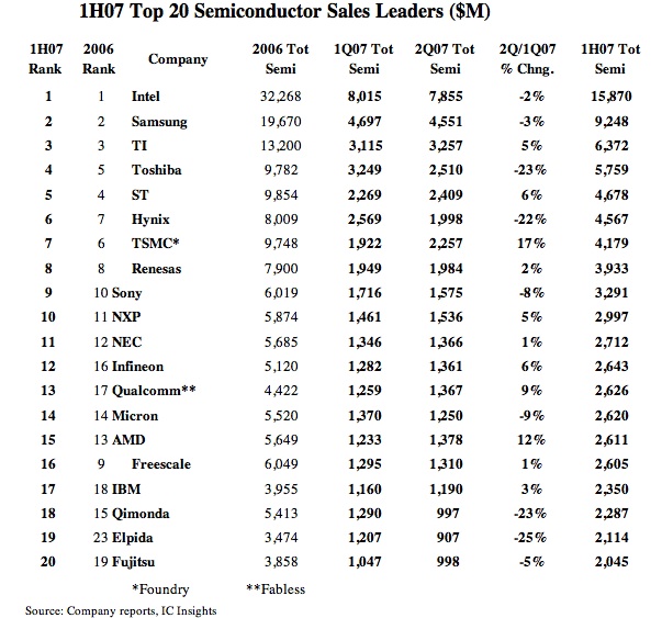
While the top three — Intel, Samsung and TI, retain their positions, ST and Toshiba have exchanged the next two positions, as have Hynix and TSMC, while Renesas remains at no. 8!
Freescale has taken a big drop from no. 9 to no. 16, while Sony, NXP and NEC gained one place each. Infineon has climbed back up to no. 12, from no. 16, while Qualcomm occupies the no. 13 position, up from no. 17. AMD dropped two positions, from no. 13 to no. 15.
Will the semicon industry see a tight year ahead? As per reports, IC Insights said that there should be a “noticeable seasonal rebound” in overall IC demand beginning in September 2007, which may cause “significant changes” in the top 20 semiconductor ranking in the second half of 2007. Wait and watch this space!
ISA initiatives bode well for semicon
When the India Semiconductor Association (ISA) started functioning from way back in Nov. 2004, it had three main objectives. These were: bringing the Indian semicon industry together; ensure that the Indian government paid enough attention to this sector; and finally, putting together a semicon policy.
ISA has since come a long way. S. Janakiraman, president and CEO – R&D Services, Mindtree, and chairman, ISA, says that the ISA is now transitioning into putting systems and processes in place.
The ISA also has three special interest groups, focusing on market research, technology and talent. The market research aspect is more in terms of reference data and in terms of opportunities.
As far as technology aspect is concerned, mixed-signal is fast becoming a reality. The process geometry of semicon has been shrinking from 90nm to 65nm and even 32nm.
Design and manufacturing used to be fairly independent earlier. However, they are fairly coupled now. All of these changes need to be addressed, according to Jani Sir. The ISA SIG on technology would be studying and recommending how to implement, keep track and stay ahead of technology.
Talent is an extremely critical area! The depth of knowledge is in danger of drying out soon! ISA feels that there is a need for a lot of faculty retraining and change in curriculum. The industry also needs to collaborate with the academia.
To address this, ISA has collaborated with the Visvesvaraya Technological University (VTU), Karnataka’s nodal body for engineering education to form the the ISA-VTU understanding. This is a comprehensive initiative, which seeks to catalyze talent generation through enhanced industry-academia interaction. The VLSI Society of India (VSI) will partner and support ISA on this initiative in specific areas.
Established in 1998, Visvesvaraya Technological University (VTU) is headquartered at Belgaum. Presently there are 120 engineering colleges affiliated to VTU. Of these, five colleges offer a post graduate degree in VLSI design and embedded software.
Key aspects of the ISA-VTU initiative are as follows:
* Creation of a Semiconductor Research Consortium-like forum for India that would foster industry-oriented research;
* Facilitation of software acquisition in identified educational institutions;
* Create and support a repository of student projects;
* Faculty development through increased industry interaction and exposure; and
* Augmenting the curriculum evolved by SMDP/ VSI/ Universities in practicals and projects
The ISA also has another program, called the Si-Quest. The Si-Quest is a pioneering semiconductor campus awareness program aimed at talent generation from a broad-based quality talent pool in India. Its nationwide campus coverage, coupled with various awareness campaigns, will attract more and better candidates towards semiconductor industry. All of these bode well for the industry.
